Imagination Announces A-Series GPU Architecture: "Most Important Launch in 15 Years"
by Andrei Frumusanu on December 2, 2019 8:00 PM ESTPPA Projections - Significant, If Delivered
Moving on, the A-Series improvements don’t mean much if we can’t put them into context in the competitive landscape.
As mentioned in the introduction, Imagination seem aware of the current PPA deficit that GPU vendor IP offers versus custom designs by more vertically integrated SoC vendors.
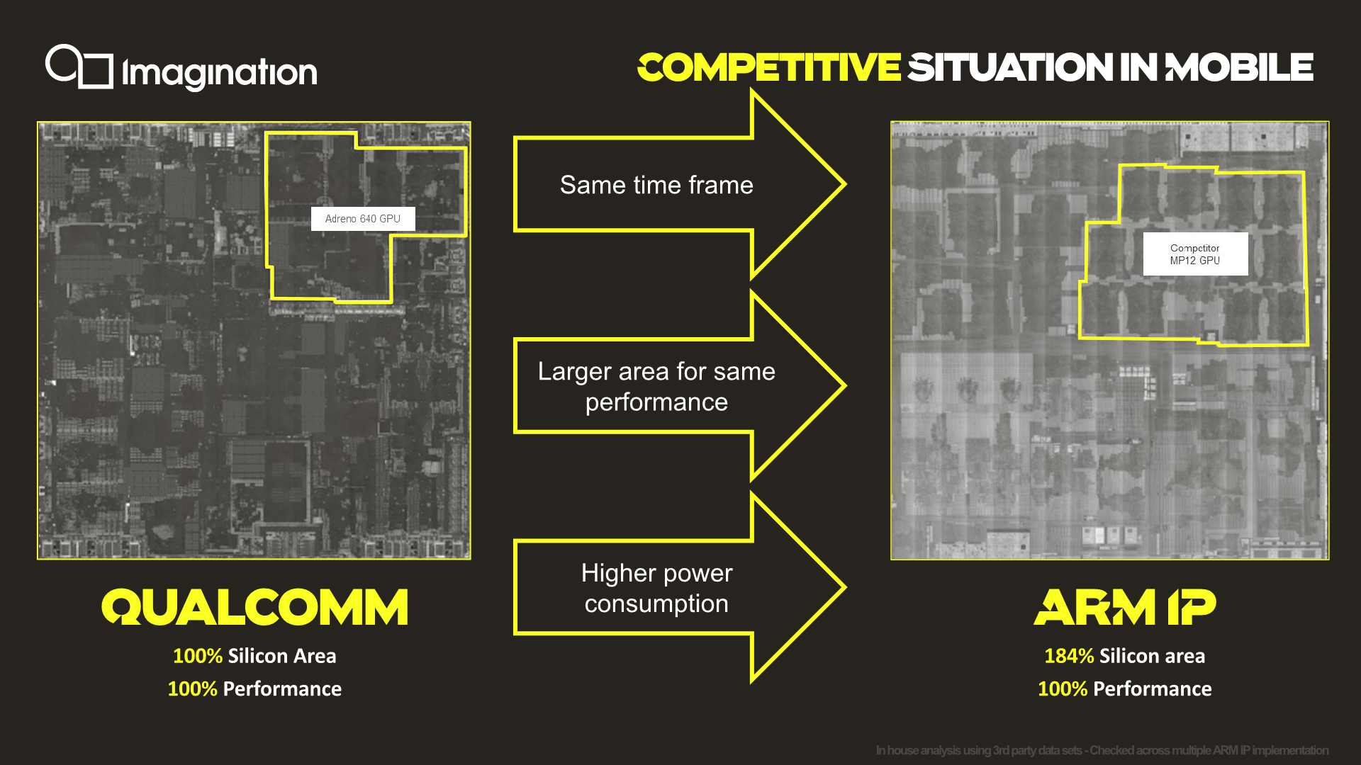
Starting off with a comparison between current generation Qualcomm GPU against an Arm GPU. Imagination didn’t specifically mention which designs we’re talking about here, but we do clearly see from the die shots that the SoCs being compared are the Snapdragon 855 and the Exynos 9820.
Here Imagination describes that for a similar performance level, Arm’s Mali GPUs are using ~184% the silicon area compared to Qualcomm’s Adreno implementation.
I do have some doubts about the validity of the comparison being made here, as these SoCs were not made on the same process node – Qualcomm's design is built on TSMC's denser 7nm process, while Samsung's Exynos uses their larger 8nm process. With that in mind, we take the metrics presented with a huge grain of salt as Imagination does say the figures are based on analysis of multiple Arm IP implementations rather than a single data-point.
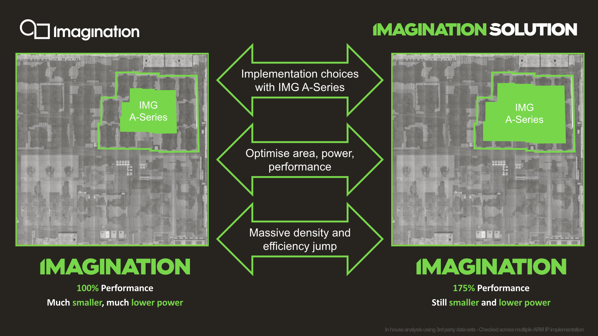
Projecting the A-Series against a current Mali-G76 implementation, targeting a performance level equivalent to current generation flagship implementations (~100fps in Manhattan 3.0), an A-Series GPU would achieve a significantly smaller GPU implementation requiring much less die area. The comparison implementation here would be an AXT-16-512 implementation running at slightly lower than nominal clock and voltage (in order to match the performance).
If a customer were to choose to use more die area to go wider and slower in clock (more efficient), while still maintaining an estimated area that would be smaller than a Mali GPU, it would roughly achieve a 75% performance advantage. The comparison here would be an AXT-32-1024 running quite far below nominal, giving it a large power efficiency advantage.
Of course, Imagination’s comparison here were made against the current generation Qualcomm and Arm GPUs, which aren't what it'll actually be competing against. Instead, by the time A-series SoCs ship, it will be competing against the next-generation Adreno as well as Mali-G77. We know Arm’s promised goals for the G77 and the improvements in performance per mm² and performance perf/W is around 1.2-1.4x, which we could generalize to 1.3x. Samsung’s upcoming Exynos 990 only promises a 20% performance increase, which is slightly below this projection. On the Qualcomm side and the upcoming Adreno generation, we’ll have to wait a few more days to be able to talk about details, but generally we expect improvements in the same ballpark.
Fortunately for Imagination, the projected PPA figures and advantages for the A-Series are high enough that they would still be notably ahead of both Qualcomm and Arm’s upcoming next generation GPUs, keeping a comfortable lead in either GPU area, or performance, depending on the configuration.
So far everything looks quite splendid – what remains to be seen if Imagination and their licensees are able to deliver on the projected figures.


143 Comments
View All Comments
extide - Monday, December 2, 2019 - link
Not exactly an announcement I was expecting to see, but quite interesting. A bit ballsy, but that's pretty much what they need right now. We'll see how it shapes up in actual products...Kishoreshack - Monday, December 2, 2019 - link
This if's & but's in the industry is soo irritatingif it releases on time it will compete well
according to its release schedule we might be at the ending cycle of Mali G77 & introduction of G78
So the performance gains are almost negligible
Pessimist9 - Wednesday, December 4, 2019 - link
But they said it! Quick! Everyone to their brokers STAT!Kishoreshack - Monday, December 2, 2019 - link
Companies overpromising & under delivering is normCOUGH *INTEL*
Seriously until the GPU hits the market
I'm seriously not interested in speculation
I'm over speculation need result's to even be excited about this
Until it is implemented in real world
the idea remains a big cloud of doubt
Cause many companies fail to stick to their release schedule
eek2121 - Tuesday, December 3, 2019 - link
Intel has real GPU products currently, they are just integrated with Intel CPUs. I definitely wouldn't say Intel is 'behind schedule' with Xe either. If you read between the lines, they are shipping 7nm products in 2021, and one of these products is a high performance GPU. As a matter of fact, despite what Intel would have you believe, I suspect that they'll keep their 10nm launches to a minimum and jump straight to 7nm. It also would not surprise me if there is a shake-up in Intel's future that causes their fab business to get spun off into it's own entity to ensure that stuff like this doesn't happen again. That last part is pure speculation though.I'd be rather curious to see how an Intel/AMD/Nvidia GPU stacks up against the Imagination one.
Also note that apparently they aren't shipping open source drivers, which right away is going to create issues for them. NVIDIA is one of the few companies that chose this route, and thus far it's caused nothing but problems for both NVIDIA and the community at large.
Korguz - Tuesday, December 3, 2019 - link
" they are shipping 7nm products in 2021, " yea right,, ill believe that, when it actually happens.." causes their fab business to get spun off into it's own entity" i doubt that would happen. 10nm is VERY late, because they tried to do to much at once, or there is another reason, who knows.. but to spin it off??? not likely
regsEx - Tuesday, December 3, 2019 - link
10 nm is DUV process of highest ever density. It's denser than TSMC 7FF DUV. 7 nm, which is generation of TSMC N3, is EUV. It's easier.TheinsanegamerN - Tuesday, December 3, 2019 - link
That's why they are now 4 years behind schedule, right?mode_13h - Wednesday, December 4, 2019 - link
Exactly.I wonder which hurt Intel more: their over-ambitious process engineers or their greedy management. Either way, while they were sputtering and cavitating, the competition blew right by them.
Their once-unassailable lead was outmatched by their own hubris.
Santoval - Tuesday, December 3, 2019 - link
Intel's 7nm node is apparently going to be slightly denser than TSMC's 5nm node (N5), *not* their 3nm node (N3). I have read about numbers in the range of ~185 million transistors (MTr) per mm^2 for TSMC's N5 and ~200 MTr/mm^2 for Intel's 7nm node. TSMC's N3, in turn, will be 255+ MTr/mm^2. Beside a quite higher density TSMC will switch to GAA-FETs at 3nm, so there can be no direct comparison anyway. In any case Intel will need to deliver 7nm first, and I strongly doubt they will manage to completely master EUV manufacturing of multiple layers by 2021.By the way, Intel's 10nm is not denser than TSMC's N7 DUV. Intel has developed three 10nm variants, for low, mid and high density. Only the high density (and highest performance) 10nm variant is slightly denser than TSMC's N7 DUV and even that was already outclassed in density by TSMC's N7 EUV (7nm+).
To my knowledge Intel employs the mid density 10nm variant for the mobile Ice Lake parts they just released, so they haven't released and aren't about to release any 10nm SoC, CPU or GPU that is denser than even TSMC's vanilla (DUV) N7. Their sole high density (100+ MTr/mm^2) 10nm parts are probably their newest Agilex FPGAs.