Intel's new Atom Microarchitecture: The Tremont Core in Lakefield
by Dr. Ian Cutress on October 24, 2019 1:30 PM ESTBeyond the Core
Nominally today’s disclosure is more about the Tremont microarchitecture than any SoC it might appear in, like Lakefield or Snow Ridge. To that end, Intel wasn’t talking about GPU support (Lakefield will have Gen11 graphics), but Intel did discuss that Tremont would be the first Atom design to fully support Intel’s Speed Shift / ACPI hardware flags, allowing for faster ramp-up and ramp-down of high-frequency operation.
Intel also stated that Tremont supports Total Memory Encryption to prevent physical attacks, Rooted Secure Boot and Boot Guard, and specific accelerator interfacing instructions. With respect to Spectre, Meltdown, and L1TF, Intel stated that Tremont will have the same protections as Cascade Lake.

We also asked Intel about module-level voltage and power control. We were told that within a quad-core module with four Tremont cores, all the cores share the same frequency plane, but each core can enter separate c-states to reduce power consumption when not in use.
Final Thoughts and Slide Deck
In the past, at least from my perspective, dealing with Atom platforms has been amusing. Atom devices typically work great for hyper-focused and optimized software that can take advantage of a latency-insensitive workload, such as networking equipment or a NAS, but for any general purpose use I find them incredibly slow. Perhaps I’m just too used to the big cores on the devices I use – but with Intel saying that Atom is being refocused on performance, it will be interesting to see how Tremont devices and other Core devices will overlap. This graph from Intel is very striking, and if you squint, it looks a lot like some of the smartphone power/performance graphs we’ve produced in the past.
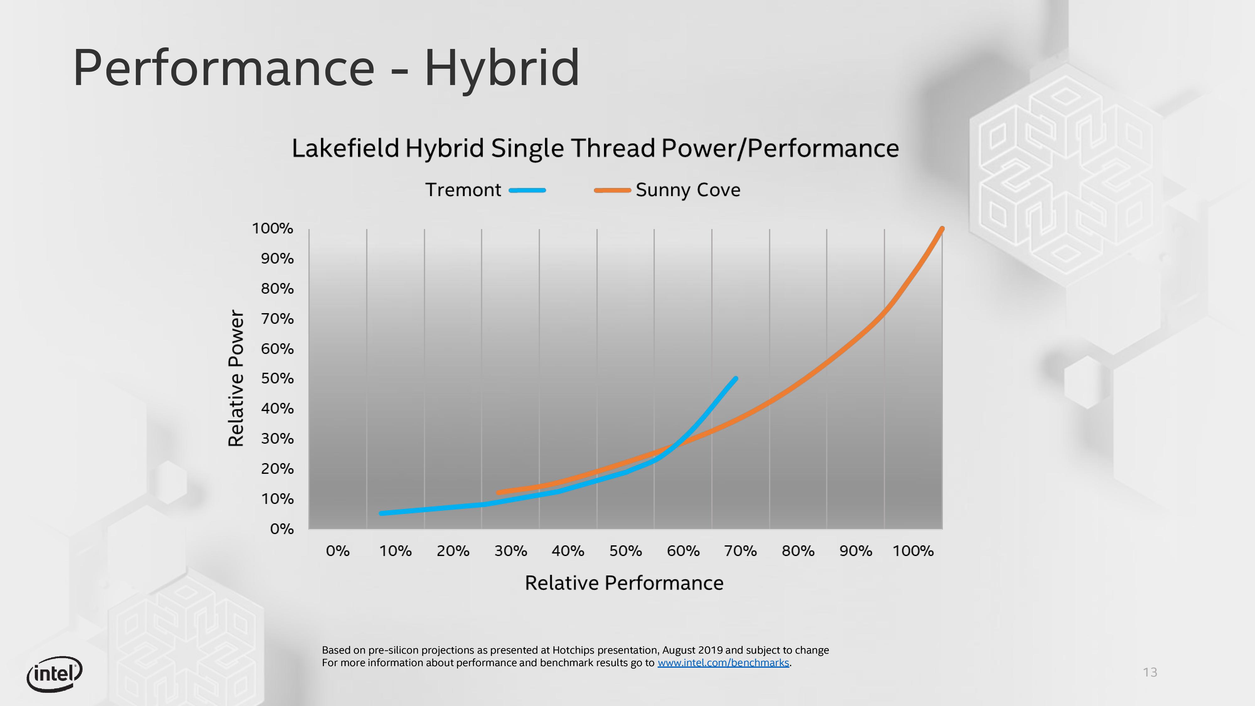
With Intel moving Core down in power to the 1.5W level, again it will be interesting to see how Tremont can play in that 2mW to 2W range that Atom has traditionally played in. The last generation Goldmont Plus devices were going beyond that, and in this power range we also have smartphone cores coming into play. After showing the slide deck to Andrei, we were discussing how a Tremont might stack up against an Arm Cortex A76, or a Kryo core. When we can get our hands on Tremont, we’ll see how they compare. When it comes to the products that Tremont is aiming for however, it still has that x86 advantage.
We did ask a few questions from Intel that we didn’t get answers to, such as die size and target frequencies. The other question to discuss is Intel’s current high-demand issues putting pressure on its manufacturing technologies. Tremont is still a low cost, low powered core, so logic may dictate that it will be a while before we see consumer chips enter the market. Ultimately Intel’s high-demand issues are around 14nm, and so far we’ve only seen Tremont discussed on Intel’s 10+ process with Lakefield and Snow Ridge. What we know about Intel’s 10nm/10+ capacity isn’t a lot, but reports vary from yields being ‘on track’ to ‘working with key OEM partners only’. Intel’s driver for 10+ right now is Ice Lake, which is coming to some premium notebook designs this year, and Lakefield has been announced for the Surface Neo. It is not known what the expected volume for the Neo will be, but it is unlikely to be large. Whether or not Tremont will see the light of day in traditional Atom Celeron and Pentium processors is another question entirely – the Goldmont Atom families have suffered while Intel’s 14nm efforts are more focused on enterprise hardware that can be sold for a much higher $$ per square millimeter. Beyond Lakefield, we might not actually see Tremont in any other consumer chip before the next generation Atom if Intel cannot get its issues sorted.
As and when we get a Lakefield device, we will put it through our tests. Stay tuned.


101 Comments
View All Comments
vladx - Friday, October 25, 2019 - link
Do you really expect Navi on future Atoms?GreenReaper - Saturday, October 26, 2019 - link
No. I was replying regarding '"the Ryzen embedded alternatives for home use".bananaforscale - Thursday, October 24, 2019 - link
Your Atom history is incorrect. The first ones were released Q2'08. Look up Silverthorne. (Yeah, I have one of the original ones.)xenol - Thursday, October 24, 2019 - link
I don't see where Ian said it started at Saltwell. Only that he mentioned the last few generations of Atom.digitalgriffin - Thursday, October 24, 2019 - link
Saltwell was the first true redesign of atom with ooe (out of order execution) iircIntelUser2000 - Friday, October 25, 2019 - link
No its not. Saltwell is a 32nm process shrink.Silvermont(Bay Trail platform) is the OoE execution Atom.
xenol - Tuesday, October 29, 2019 - link
The SoC implementation of Atom started with Saltwell. So if Ian's context was the SoC implementation, then starting at Saltwell makes sense.Namisecond - Friday, November 1, 2019 - link
If by 'SoC', you mean the tablet and phone chips, I think that was Silvermont, not Saltwell.maroon1 - Thursday, October 24, 2019 - link
Does this mean that all five cores can be used together by the application ??I think this will show 6 threads in task manager (cause sunny core has two threads, + 4 Atom cores)
skoo - Thursday, October 24, 2019 - link
Stay away from it (if it ever really comes out). I got left high and dry by intel with their previous atom foray into tablets. They decided it was a failure and just stopped supporting the chip (no more drivers for os upgrades) so I am stuck with a tablet with android 6.01 on it