Intel's new Atom Microarchitecture: The Tremont Core in Lakefield
by Dr. Ian Cutress on October 24, 2019 1:30 PM ESTA Wider Back End
Moving beyond the micro-op queue, Tremont has an 8 execution ports, filled from 7 reservation stations.
The only two ports using a combined reservation station are the address generator units (AGUs) - this is in stark contrast to the Core design, which in Sunny Cove uses a unified reservation for all integer and floating point calculations and three for the AGUs. The reason that Tremont uses a unified reservation station for the two AGUs, also backed by extra memory for queued micro-ops, is in order to supply both AGUs with either 2x 16-byte stores, 2x 16-byte loads, or one of each. Intel clearly expects the AGUs on Tremont to be fairly active compared to other execution ports.

On the integer side, aside from the two AGUs, Tremont has 3 ALUs, a jump port, and a store data port. Each ALU supports different functions, with one enabling shift functions and another for multiplication and division. Compared to core, these ALUs are extremely lightweight, and Intel hasn’t gone into specifics here.
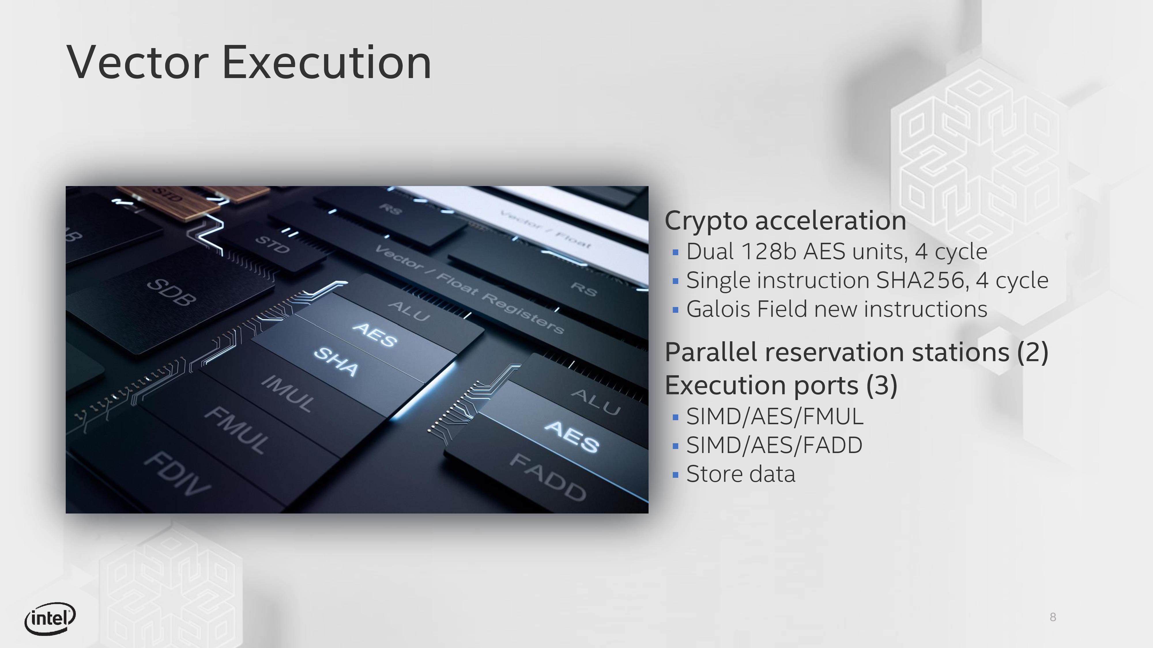
On the floating point side, we are a little bit more varied – the three ports are split between two ALUs and a store port. The two ALUs have one focused on fused additions (FADD), while the other focuses on fused multiplication and division (FMUL). Both ALUs support 128-bit SIMD and 128-bit AES instructions with a 4-cycle latency, as well as single instruction SHA256 at 4-cycles. There is no 256-bit vector support here. In order to help with certain calculations, GFNI instruction support is included.
There is also a larger 1024-entry L2 TLB, supporting 1024x 4K entries, 32x 2M entries, or 8x 1G entries. This is an upgrade from the 512-entry L2 TLB in Goldmont.
New Instructions
As with any generation, Intel adds new supported instructions to either accelerate common calculations that would traditionally require lots of instructions or to add new functionality. Tremont is no different.
| TITLE | |||||
| AnandTech | Tremont | Goldmont Plus |
Goldmont | Airmont | Silvermont |
| Process | 10+ | 14 | 14 | 14 | 22 |
| Release Year | 2019 | 2017 | 2016 | 2015 | 2013 |
| New Instructions | CLWB GFNI ENCLV CLDEMOTE MOVDIR* TPAUSE UMONITOR UWAIT |
SGX1 UMIP PTWRITE RDPID |
RDSEED SMAP MPX XSAVEC XSAVES CLFLUSHOPT SHA |
SSE4.1 SSE4.2 MOVBE CRC32 POPCNT CLMUL AES RDRAND PREFETCHW |
|
(When asked what other new instructions are supported, Intel stated to look at the published documents about future instructions. When it was pointed out that those documents weren’t exactly clear and that in the past Intel hasn’t spoken about future designs, we were not afforded additional comments.)
When we get hold of a Tremont device, we’ll do a full instruction breakdown.


101 Comments
View All Comments
eddman - Saturday, October 26, 2019 - link
MP4 is a container, not a codec.Alien959 - Friday, October 25, 2019 - link
I am reading this article on goldmont + powered laptop. While definitely is not a speedster, the hardware is perfectly usable for light tasks like internet browsing, text editing I even did some 1080p edits in premiere and some modeling in SketchUp pro. It handles the tasks fine. The rest of the hardware is a ssd and 8 gb of ddr4 ram. The main reason what makes the system usable is that the GPU is supported in both programs, and that alleviates the speed of weaker cores on the CPU side.Bigos - Friday, October 25, 2019 - link
> The two ALUs have one focused on fused additions (FADD), while the other focuses on fused multiplication and division (FMUL).Did you mean *float* instead of fused? The only thing that comes to my mind when you say "fused" is FMA: fused multiply-accumulate.
Also, in the "New Instructions" section the table is titled "TITLE", which sounds amusing but is probably a left-over.
mode_13h - Saturday, October 26, 2019 - link
Yeah, this was also mentioned above. You are correct, as I said in my reply to @ternnence.snakyjake - Friday, October 25, 2019 - link
If it works for HTPC, decodes HEVC efficiently, low power, low heat, fanless, then I'll buy it.Namisecond - Friday, November 1, 2019 - link
The current Goldmont+ chips already do all that.ksec - Saturday, October 26, 2019 - link
Not useful without pricing. In terms of absolute numbers in both Performance and power, ARM or POWER has readily available solutions.Elstar - Saturday, October 26, 2019 - link
The dual frontend decoders seem ideal for SMT performance. I'm surprised they don't have that option for those that want it.TomWomack - Sunday, October 27, 2019 - link
'1.5 MB will be a 12-way design, while 4.5 MB will be an 18-way design. (We therefore assume that a 3.0 MB L2 will be 15-way'1.5MB 12-way would be 12 256kb blocks; 4.5MB 18-way would be 18 512kb blocks; 3.0MB would be either 24-way with 256kb blocks or 12-way with 512kb blocks, almost certainly the latter
AshlayW - Sunday, October 27, 2019 - link
Intel's new SoC design with "low power" and "high power" cores, akin to the big.LITTLE from ARM, is actually pretty awesome. I'll give them credit where it's due, Sunny Cove, and Tremont are shaping up to be fantastic architectures - for low power mobile, an area where I'd love to see more super tiny low power x86 devices, as I have grown quite fond of my HP envy X360, even though it has the comparatively less efficient Raven Ridge silicon in it (2500U).It's just a shame they won't have anything interesting on the desktop. I'll tell you what, Intel. If you want my custom, get these ULP chips into something like a One mix Yoga 3, and I might even buy it. Now imagine playing Warframe, on the go, on a device I can slip in my pocket with a wireless Xbox Controller in the other one. Make it happen.