Intel 65nm and Beyond (or Below): IDF Day 2 Coverage
by Kristopher Kubicki on September 9, 2004 9:26 AM EST- Posted in
- Trade Shows
Lithography
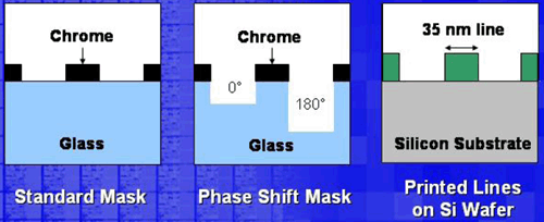
Moving to a 65nm transistor requires a 65nm lithography process. We are already seeing devices being built into silicon with features smaller than the wavelength of the light used in the lithography process. As it will be somewhere near 2009 before Intel has their EUV (13nm light wavelength) technology up and running, working with such small features requires some special masking tricks.
At this level, engineers must take into account the fact that light displays properties of both particles and waves. In order to create the situation where a particle of light has a high probability of hitting such a small section of photoresist covered silicon, special masking techniques need to be used to manipulate the wave.
Though it's not the same thing, anyone who has access to a laser can see how a light wave can be manipulated. Just take a piece of paper and cut two vertical slits that are close enough together so as to fit within the radius of the laser pointer beam. Find a dark room, stand a few feet from a wall, and shine your laser through the slits in the paper. What will be seen is a series of vertical lines which represent the interference pattern of the light waves passing through each slit. Well, that's the explanation if we don't try to talk about it on the quantum level.
Using similar properties exhibited by light (though not exactly the same as our example), Intel has devised technology they call Alternating Phase Shift Masks in order to etch extraordinarily small features into a silicon integrated circuit for 65nm fabrication.
Moving to 32nm fabrication, we think Intel will be forced to move to EUV (both the process technology roadmap and the move to 13nm wavelength lithography will occur circa 2009). But until then, and even beyond, advanced masking techniques will enable photolithography to keep up with the ever decreasing size of transistors on silicon.


21 Comments
View All Comments
mikecel79 - Thursday, September 9, 2004 - link
Great article on Intel's technology but why nothing about the dual core P4 they showed running on a 915 board yesterday?From the ZDnet article at http://zdnet.com.com/2100-1103_2-5356703.html
"Like the current Pentium 4, Intel's dual-core desktop chip is built on the NetBurst architecture and fits into motherboards using Intel's 915 Grantsdale chipset. But Siu declined to provide many details on the dual-core demonstration chip, which he described as an engineering prototype.
"It is real silicon running on a standard 915 platform," Siu said. He wouldn't comment on whether it has the 64-bit memory extension technology, called EM64T."