Intel 65nm and Beyond (or Below): IDF Day 2 Coverage
by Kristopher Kubicki on September 9, 2004 9:26 AM EST- Posted in
- Trade Shows
Silicon and Transistor Technology
Advances in lithography technology have only been half of the battle in fulfilling Moore's law. In fact, silicon and transistor technology itself has undergone radical changes in the last couple years (particularly with technology like strained silicon). Putting more transistors on a processor recently has had more to do with increasing cache size rather than increasing logic on the CPU. Advances in lithography and gate technology dramatically increase our density of other components such as SRAM - the building blocks of cache memory.
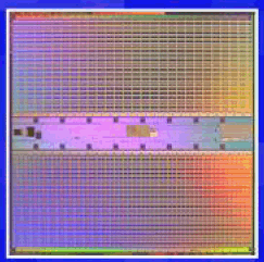
DRAM effectively utilizes one transistor per cell, allowing high densities but unfortunately operating at low speeds. SRAM utilizes six transistors per cell in a flip flop configuration, lowing density but allowing operation at several GHz. Below, Intel demonstrates a 110mm2 SRAM module with a 70Mbit capacity (over 500 million transistors). This is less than a modern BGA module can handle, but consider the SRAM module can operate several GHz faster than any DRAM module with ease.
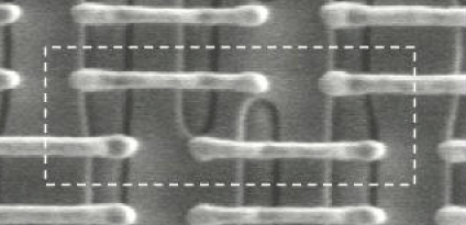
You can see an actual SRAM cell in the image below. The white dash outlines a cell with an area about 0.57um2.
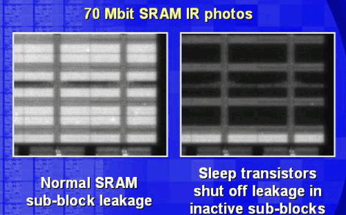
Simply designing more and more transistors on a chip does not make sense if thermal issues bog down the true capabilities of the processor. We spotted one new technology that did not receive a lot of attention during the presentations; the introduction of sleep transitors. Sleep transistors act as miniature controllers to an SRAM bank, throttling power during operating to reduce leakage. The sleep transistors themselves do not sleep, but rather the transistors they control do.
Further advances at Intel, like trigate transistors will essentially place transistor interconnects on a 3D grid instead of a 2D one - allowing for much higher densities without revamping lithography or gate size.
Intel already uses low-k dielectrics between their metal layers to reduce capacitance They use a Carbon Doped Oxide (CDO) for this, though they weren't specific about what oxide they are using for this. This will continue into 65nm, and strained silicon will see some slight revisions as well. Currently their silicon germanium (PMOS) and nickel silicide (NMOS) strained silicon gives about a 20% average improvement in transistor drive current, but Enhanced Strained Silicon (as they are calling it) promises a 30% average improvement.
At this point in time, Intel did not discuss exactly what makes their next step in strained silicon "enhanced", but they were fairly tight lipped about their original implementation before it hit the market.


21 Comments
View All Comments
drwho9437 - Friday, September 10, 2004 - link
Eskimo I was jus being sloppy in my language. As I progressed. Its good to know I'm not totally nuts. The resists will be a problem because of chain length. I mean for positive resists it seems ovious as it seems to be the ratio of the native to the broken resist chain length that would matter (there solublity). For a negative resist I guess you could somehow have some very simple and short chain somehow but I would think it would still need to be of the order of nm in length. I think it will be interesting if intel or someone else can reach high yeilds on structures of 5-10nm size. That would make SETs or other quantum devices useable in the millions.KristopherKubicki - Friday, September 10, 2004 - link
ceefka: Intel is actually moving in the other direction - particularly for server products. The Memory controller is in fact getting its own tunnel on chipsets like Twin Castle. I suspect this is being done so that they can incorporate multiple memory controllers on a single motherboard.Kristopher
ceefka - Friday, September 10, 2004 - link
Great article, Kristopher.7 + 17 Right on! Seems like all they're doing is shrinking, more cache and pumping the FSB.
Where is that on die memory controller?
It doesn't seem like much of an animal if you keep it in a cage. What they're doing at Intel is great in itself, but it needs something extra.
Eskimo - Thursday, September 9, 2004 - link
#13/#14, You are correct we are now entering the arena where the actual polymer chains which make up our resists are approaching some of the features that are being printed on the wafers. As for etching keep in mind that we don't actually etch the resist. Resist after exposure is developed away in an aqueous solution. The remaining resist serves as a mask for the underlying material either protecting from ion bombardment or etches. The standard etch for today's high aspect ratio features is Reactive Ion Etching (RIE). The 193nm resists in use in leading edge lithography do not have the same etch protection capabilities that were present in DUV(248nm) and i-line(365nm) resists. A new challenge for resists is posed by the upcoming widespread adoption (even Intel might come around) of immersion lithography where the resist will be directly exposed to water in the scanner.As for the article itself, it seems to suggest that Intel came up with the idea of phase shift masks. When in fact they were developed in the late 70's and first put into use in the early 90's by a variety of companies. The only real news on this front is that to reach 65nm on 193nm dry systems you will definately need alternating aperature phase shift masks like the diagram describes which are very costly.
As for the statement saying Intel did not specify what sort of oxide they are doping with carbon for their low-k dielectric it is Silicon Dioxide. Since SiO2 is so prevalent in silicon processing and so well understood we often just refer to it simply as oxide. If it was in fact another material oxidized that would've been specifed (e.g. Aluminum Oxide).
mkruer - Thursday, September 9, 2004 - link
#7 Read again what I wrote, I mentioned nothing abut the SPEED, working faster =! Speed in MHz which you are apparently inferring. I was simply stating that obvious that Intel solution for the majority of its problems is to simple through more cache at it.GodsMadClown - Thursday, September 9, 2004 - link
I remeber going to a talk on the Chandra X-Ray telescope and hearing about all the craziness with mirrors that they had to go through to get the optics to work. I guess that Intel could do the same thing, but It's just getting crazy. No real content, but to make everyone aware that when you deal with EUV radiation, optics get very complex.stephenbrooks - Thursday, September 9, 2004 - link
I'm pretty sure that on the last page it should be "line width" going to 0.7x every two years, not line LENGTH! Total line length on a chip should increase 1.4x every two years because they're packing it in smaller.drwho9437 - Thursday, September 9, 2004 - link
To clarify, I mean you have to etch the resist, dry or wet, you have to do it and that has some limit, but I don't know what it might be or even what kind of etching big fabs use.drwho9437 - Thursday, September 9, 2004 - link
Humm. Aren't we going to hit the limit of resists soon? I mean the resists I know about for ebeam lithography have resolution of something like 8nm. Intel is going to do 23 with photolithography, that's impressive, you can always go to x-rays if all it was was a matter of making the photon wavelength sorter but what about the chemistry? (I'm not a chemist, I'm a physicist/EE)ncage - Thursday, September 9, 2004 - link
I read the other post and thats what i used as my reference to spell it. Dumb idea i guess ;)