The Ice Lake Benchmark Preview: Inside Intel's 10nm
by Dr. Ian Cutress on August 1, 2019 9:00 AM EST- Posted in
- CPUs
- Intel
- GPUs
- 10nm
- Core
- Ice Lake
- Cannon Lake
- Sunny Cove
- 10th Gen Core
Cache and TLB Updates
One of the biggest changes in the new Sunny Cove core is the cache hierarchy. Throughout most of the last decade, Intel has kept the same cache configuration among its server cores with very few changes, aside from improving the micro-op cache through Sandy Bridge today, but with Sunny Cove, we get some key updates.
From our microarchitecture disclosure article, we know that Sunny Cove brings with it an increased L1 data cache, as well as a doubled L2 cache, from Skylake. With this comes more associativity as well.
| Core Cache Comparison | ||||||
| Sunny Cove |
AnandTech | Cannon Lake |
Skylake | Sandy Bridge |
AMD Zen 2 |
|
| 48 KB 12-way |
L1-D | 32 KB 8-way |
32 KB 8-way |
32 KB 8-way |
32 KB 8-way |
|
| 32 KB 8-way |
L1-I | 32 KB 8-way |
32 KB 8-way |
32 KB 8-way |
32 KB 8-way |
|
| 512 KB 8-way |
L2 | 256 KB 4-way |
256 KB 4-way |
256 KB 8-way |
512 KB 8-way |
|
| 2 MB 16-way |
L3/core | 2 MB 16-way |
2 MB 16-way |
2MB 16-way |
4 MB 16-way |
|
| 2304 | uOp Cache | 1536 | 1536 | 1536 | 4096 | |
I’ve also included the size of the micro-op cache in this comparison, because we understand that the L1-I and the micro-op cache are typically located next to each other in the die design – increasing the size of one typically means limiting the size of the other, however given that both of them work to accelerate the same types of data, it is important to find the right balance: AMD for Zen 2 decided to halve the L1-I and double its associativity, and then double the micro-op cache from 2k to 4k entries. For Sunny Cove, Intel has increased the L1-D by 50%, but also increased the micro-op cache by 50%, taking advantage of the second generation 10nm process.
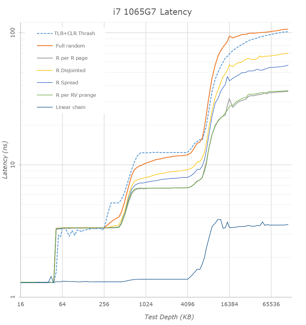
In the above latency graph comparison, we can notably see the new increased cache capacities. The L1’s increase from 32KB to 48KB is well visible, as well as the L2 increase from 256KB to 512KB.
On the part of the L2 it’s interesting to see that again the new core’s TLB structures don’t quite cover the whole capacity of the L2 and that’s why the latter half of the L2 has worse access latencies for L1D TLB miss patterns.
L3 latencies look similar, however we’ll dwell into that just in a bit. The DRAM latencies of course are apples and oranges in this case as Intel’s new LPPDR4X memory controller in the new ICL part doesn’t have a counter-part we can compare to, but as expected the memory latency is notably worse than a desktop part so no big surprises there.
What’s rather disappointing however is that we’re not really seeing any kind of change to the prefetchers and our access patterns between the two microarchitectures look identical. We had expected Intel to improve in this regard, but alas it seems, at least for our test cases, there’s been no improvements.
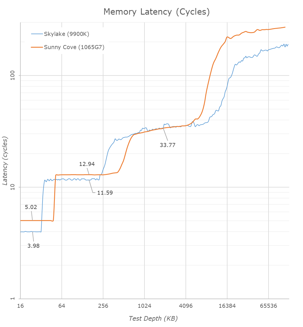
One of the major balancing acts with cache sizes is also cache latency. The bigger the cache, the longer it takes to retrieve data from it – increasing associativity can do this as well. Intel for the longest time has cited a 4-cycle latency to its L1 cache, and a 12-cycle latency to its L2 cache. This changes, in quite a substantial way.
| Core Cache Latency (in cycles) | ||||||
| Sunny Cove | AnandTech | Cannon Lake |
Skylake | Sandy Bridge |
AMD Zen 2 |
|
| 5 | L1 | 4 | 4 | 4 | 4 | |
| 13 | L2 | 12 | ~12 | 12 | 12 | |
| 30-36 | L3 | 26-37 | 34 | |||
Due to the increase in the L1 cache, that 4-cycle latency is now a 5-cycle latency. Intel is hoping that its double L1 store bandwidth will help hide that latency, however adding 20% latency onto every data fetch is a heavy hit to take. This is why a lot of the rest of the core is also beefed up, so work can still continue to cover for this extra cycle. It is worth noting that Intel’s Atom cores in the past had an L1 latency of 3 cycles, however they have also since moved to 4-cycle.
The L2 also changes, from 12 cycles to 13 cycles. You can’t double a cache for free, and it is interesting to note here that now AMD and Intel share the same L2 cache size and the same associativity, however AMD has a cycle advantage on Intel. This has a knock on effect for L3 cache latency too, which has increased from ~26-37 cycles to ~30-36 cycles on Intel, from Skylake. The latency here isn’t uniform because the cache isn’t uniform, and accessing non-local L3 slices comes with a latency penalty, as say opposed to AMD’s uniform latency L3.
One of the biggest additions Intel was keen to make in our Sunny Cove microarchitecture disclosure is the increase in the L1 bandwidth. Based on our testing, Skylake’s L1 data cache was capable of 2x32-byte read and 1x32-byte write per clock. For Sunny Cove this has increased, but it gets a bit more complicated. In one clock Sunny cove can perform 2x64-byte reads and either 1x64-byte write, or 1x32-byte write, or 2x16-byte writes. So both reads and writes, at peak, have doubled with bit width, with the write configurations being a bit more complex.

We can see the direct effects of the bandwidth change in our bandwidth tests. The L1 store bandwidth is extremely evident as it measures in at 222GB/s on the ICL part, while only reaching 139GB/s on the 28% higher clocked 9900K. If we normalise for frequency, we indeed see a doubling of the store bandwidth of the new core.
The L2 cache bandwidth looks unchanged from Skylake – the part here lags behind with an equal amount to the frequency difference. Surprisingly, the L3 bandwidth fares quite well here and is almost at parity to the desktop 9900K even though the frequency difference. The DRAM bandwidth is inferior on the ICL mobile chip, but again that’s to be expected due to the apples and oranges DRAM architecture comparison.
Moving on to the TLB configurations, and it turns out that Intel has moved where this data is stored. This data is typically stored in CPUID.02h, however it is now found in CPUID.18h, and the info between different page sizes and capabilities is now given as subdivisions. The TLBs look as follows, and broken down into configurations:
| Sunny Cove TLB | |||
| AnandTech | Type | Entries | Associativity |
| L1-D | 4K | 64 | 4-way |
| L1-D | 2M | 32 | 4-way |
| L1-D | 1G | 8 | full |
| L1-I | 4K+2M | 8 | full |
| L1-I | 4K+2M+1G | 16 | full |
| L2 | 4K+2M | 1024 | 8-way |
| L2 | 4K+1G | 1024 | 8-way |
This means that for 4K and 2M L1-I entries, there are a total 8+16 = 24 possible, but only 16 1G possible. For 4K L2 entries, there are 1024 + 1024 = 2048 entries possible, however only 1024 each of 2M/1G are possible. The peak numbers align with what Intel has told us in our microarchitecture disclosure, however it is good to dive into what is possible.


261 Comments
View All Comments
The_Assimilator - Thursday, August 1, 2019 - link
Not to mention that all Intel's CPU fabs have been on 14nm for so long that the capital costs are long paid off.I think we will see ICL on desktop via 14nm, simply because Intel can't afford to not compete with Zen 2. We won't get the full 20% IPC uplift because Intel will have to spend some of that to deal with 14nm's power/heat issues at high frequencies, but even a 10% bump would be enough to decisively regain the performance crown from Zen 2.
dwbogardus - Thursday, August 1, 2019 - link
Pretty much every major architectural change and most every process shrink Intel has made over decades has initially resulted in only very modest improvements. But over time, as volumes and yields improved, they did process tweaks and minor die spins, and the yield had higher frequencies gradually improved. The very first Pentiums/Pentium Pro's struggled to out-perform the then-fastest 80486DX2-66's, on then-existing applications. There has been a slow, by consistently steady over decades improvement in IPC, and generally in frequency, with temporary setbacks in frequency at each new process introduction. But over time, they always ratchet up, with the cumulative effect over the years being very dramatic. While we're all surprised and disappointed that it has taken as long as it has for Intel to get 10 nm out, no one should be surprised that initial yields and frequencies are very modest. They always are, but they always improve, and in the case of 14 nm, they managed to improve them so much that they have been hard to let go of and move on from. In fact, 14 nm is still the best fit for some applications, and will remain so for so time.nevcairiel - Thursday, August 1, 2019 - link
Unfortunately Intel decided a long time ago to not bother to backport Ice Lake to 14nm. Ice Lake had been "done" for years, basically, afterall.On the other hand, they did say that in the future, and with growing uncertainty of process gains, they want to develop architectures in a manner more independent from the actual process, so hopefully Ice Lake is the last µarch thats very tightly married to its process.
hbsource - Thursday, August 1, 2019 - link
Was that an HST reference with the Good Thing trademark?konbala - Thursday, August 1, 2019 - link
How does Integer Scaling working out to be? Really curious, can’t wait to play games smoothly at low res.Alistair - Thursday, August 1, 2019 - link
Kind of what we were expecting, which isn't much. 3 percent ST gains. Can now play AAA titles at 720p at 19fps... not exciting. We don't even get an upgrade from 4 to 6 cores at the same price, like what happened in the desktop. Terrible if you ask me. Guess I'll be keeping my laptop another year.twotwotwo - Thursday, August 1, 2019 - link
Curious if this ends up a return to Intel's old routine or if there's still constrained supply, etc. In particular, the longer 10nm server chips take to arrive, the longer AMD could grow off server revenue.Two tick+tocks a few weeks apart! Busy times for AT, heh.
trivik12 - Thursday, August 1, 2019 - link
Obviously AMD Loons are nervous. Intel will ultimately figure out process issues and then AMD will be back where they were few years back.Alistair - Thursday, August 1, 2019 - link
Maybe you didn't understand what you just read. This is the smallest improvement in CPU performance that Intel has had for years in mobile. Go look at that image again.https://images.anandtech.com/doci/14664/Blueprint%...
maroon1 - Thursday, August 1, 2019 - link
The iGPU gain is massive