The Samsung Galaxy S10+ Snapdragon & Exynos Review: Almost Perfect, Yet So Flawed
by Andrei Frumusanu on March 29, 2019 9:00 AM ESTThe Snapdragon 855 SoC - A Recap
Although the Galaxy S10 is the first Snapdragon 855 device we’re reviewing, Qualcomm’s new chipset shouldn’t come with any major surprises. We had the opportunity to conduct an extensive and in-depth performance preview back in January at CES, which answered a lot of our initial questions about Qualcomm's new flagship SoC. Indeed the Snapdragon 855 largely met our expectations: The new CPU on the new process node performs very similarly to the other 7nm + A76 design we've already seen – the Kirin 980 chipset from HiSilicon – with only minor differences on the CPU complex.
Where Qualcomm strongly differs from the competition is in in the auxiliary accelerator blocks such as GPU, DSP and the new tensor units. Let’s go over the specifications again:
| Qualcomm Snapdragon Flagship SoCs 2018-2019 | |||
| SoC |
Snapdragon 855 |
Snapdragon 845 | |
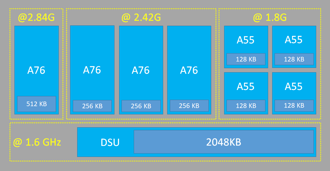
| CPU | 1x Kryo 485 Gold (A76 derivative) @ 2.84GHz 1x512KB pL2 3x Kryo 485 Gold (A76 derivative) @ 2.42GHz 3x256KB pL2 4x Kryo 485 Silver (A55 derivative) @ 1.80GHz 4x128KB pL2 2MB sL3 @ 1612MHz |
4x Kryo 385 Gold (A75 derivative) @ 2.8GHz 4x256KB pL2 4x Kryo 385 Silver (A55 derivative) @ 1.80GHz 4x128KB pL2 2MB sL3 @ 1478MHz |
|
| GPU | Adreno 640 @ 585MHz | Adreno 630 @ 710MHz | |
| Memory Controller |
4x 16-bit CH @ 2092MHz LPDDR4X 33.4GB/s 3MB system level cache |
4x 16-bit CH @ 1866MHz LPDDR4X 29.9GB/s 3MB system level cache |
|
| ISP/Camera | Dual 14-bit Spectra 380 ISP 1x 48MP or 2x 22MP |
Dual 14-bit Spectra 280 ISP 1x 32MP or 2x 16MP |
|
| Encode/ Decode |
2160p60 10-bit H.265 HDR10, HDR10+, HLG 720p480 |
2160p60 10-bit H.265 720p480 |
|
| Integrated Modem | Snapdragon X24 LTE (Category 20) DL = 2000Mbps 7x20MHz CA, 256-QAM, 4x4 UL = 316Mbps 3x20MHz CA, 256-QAM |
Snapdragon X20 LTE (Category 18/13) DL = 1200Mbps 5x20MHz CA, 256-QAM, 4x4 UL = 150Mbps 2x20MHz CA, 64-QAM |
|
| Mfc. Process | TSMC 7nm (N7) |
Samsung 10nm LPP |
|
The Snapdragon 855 is Qualcomm’s first SoC powered by Arm’s new Cortex-A76 CPU core, which we also saw in the Kirin 980. Qualcomm still makes use of Arm’s “Built on Cortex Technology” license, where it requests changes to the CPU IP to be delivered by Arm. The end product ends up marketed as a Kryo CPU – in the case of the Snapdragon 855 the new “Kryo 485” CPU.
In past iterations it’s not always been clear exactly what changes Qualcomm had made to the CPU cores, so it was a surprising and much welcomed change to have the company actually provide concrete examples in the case of the new Snapdragon 855 CPU cores: The two big disclosed changes are an increase of the core’s reorder buffer from 128 entries to a higher, unspecified amount, as well as tuning the prefetchers to better work with floating point workloads.
The one thing that makes the Snapdragon 855 unusual though is the new physical CPU configuration. Both the Kirin 980 as well as the Snapdragon 855 both contain four Cortex A76 cores, however the two companies implement these in two completely different ways.
While HiSilicon had opted for a 2+2 core configuration where one pair clocks up to 2.6GHz and the other only reaches 1.92GHz, Qualcomm opts to go with a 1+3 setup. Under Qualcomm's setup one core is clocked up to 2.84GHz, and meanwhile the other three cores reach up to 2.42GHz. While at first glance this makes sense, things get confusing when accounting for the fact that the Snapdragon still only has a single voltage plane for all four CPU cores, whereas the Kirin’s CPU pairs both have their dedicated rails.
Qualcomm has explained that this was a deliberate choice which took into account the actual benefits, as well as (most importantly) the costs of the platform. Having an additional voltage rail means your PMIC needs an additional buck converter and you need to have additional inductors and capacitors on the motherboard, a cost not only in terms of actual component costs but also in terms of valuable PCB space.
What this means is that the power difference between the two CPU groups is much less than one would expect, but most interestingly it will be a difference that is solely dictated by the different physical implementations of the two cores.
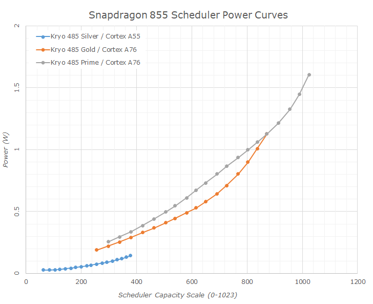
In later sections we’ll address the efficiency difference between the two groups of cores, and one thing that was surprising is that the “middle” cores weren’t that much more efficient than the “prime” core. I extracted the power curves out of the scheduler, as dictated by Qualcomm, and this reveals a bit more information and clarification.
What we see is that the middle “Gold” cores’ power curve shape is shifted down towards lower power, meaning it starts growing at an exponential rate earlier than what we see on the “Prime” core. This would explain why at peak performance, the efficiency difference between the two cores is minor. When we look at the middle frequency points in particular though, we see what this power difference is more notable and actually at its greatest point does represent up to 20% lower power on the mid cores compares to the prime core.
Qualcomm also differentiates the large CPU cores by their cache configuration: The Prime core gets 512KB of L2 while the middle cores make due with 256KB. The Cortex A55’s have the usual 128KB and Qualcomm clocks them conservatively at 1.78GHz.
Finally, the DSU’s L3 cache comes in at 2MB. A big question I had is exactly how fast Qualcomm had clocked the cache at, and the answer is 1.6GHz. This represents a slight increase over the 1478MHz of the L3 cache found in the Snapdragon 845.
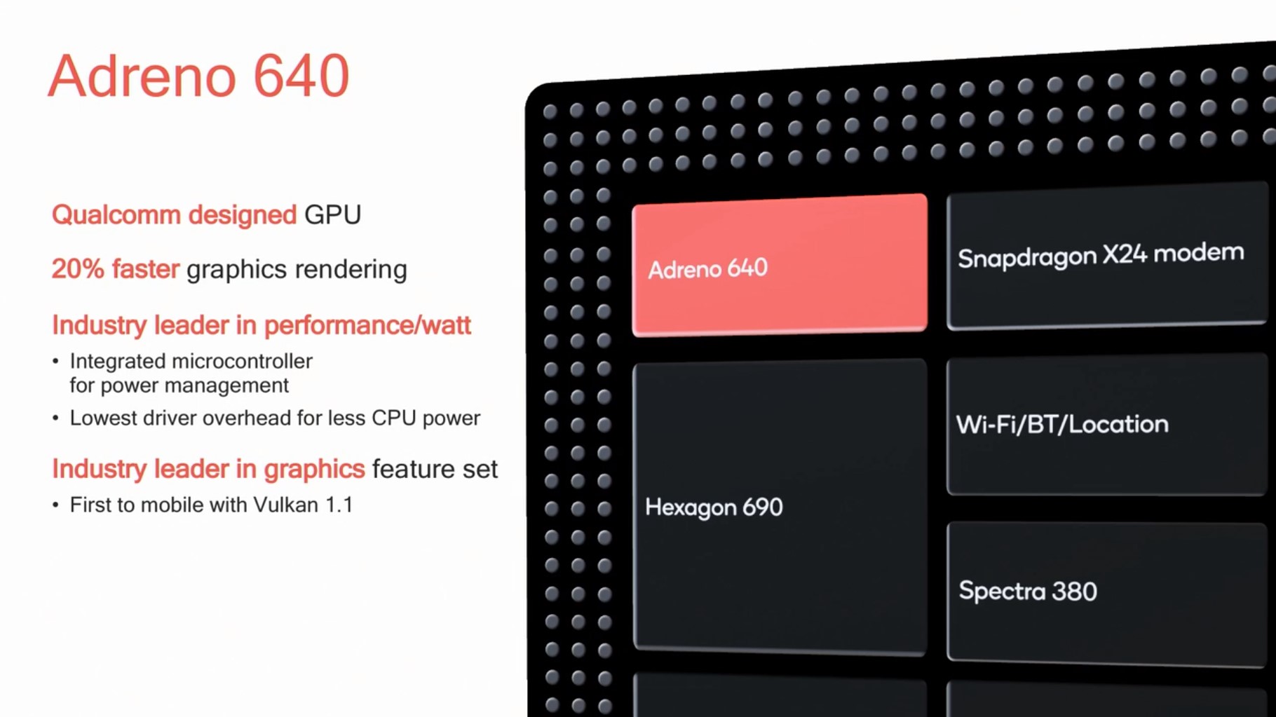
Other large architectural changes in the Snapdragon 855 are the new Adreno 640 GPU. Here Qualcomm supposedly has increased the execution units by 50% - yet only advertise a 20% boost in performance. The explanation here lies in the clock frequency of the new GPU. The Adreno 640 in the Snapdragon 855 runs at only 585MHz, markedly slower than the 710MHz of the Adreno 630. I suspect that Qualcomm saw some of the increasing power usage of the higher clock frequencies and decided it’s better to go wider and slower. Indeed, we’ll see that the Snapdragon 855 has managed to reduce power usage in 3D workloads ever so slightly compared to the Snapdragon 845 – something which should definitely help thermals and sustained performance.
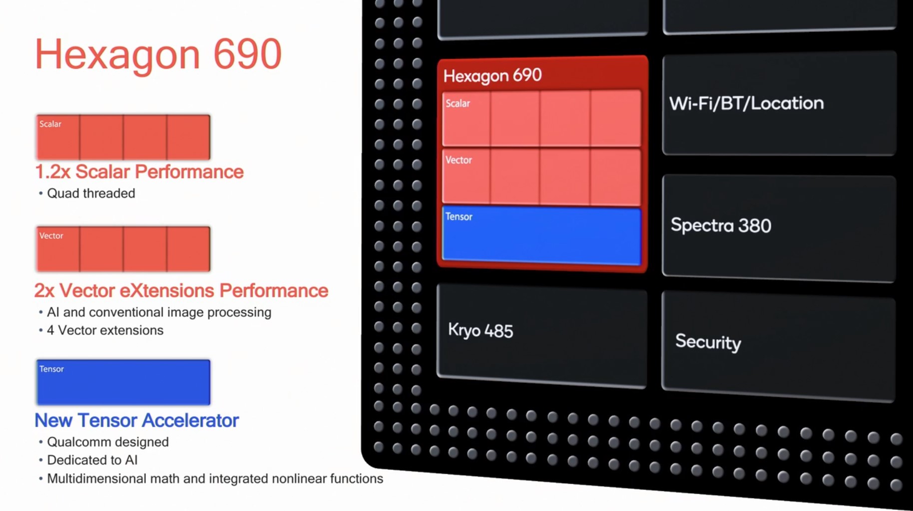
Finally, the new Hexagon 690 DSP block has seen its biggest change in several years. Scalar performance has gone up by 20% through microarchitectural and clock frequency bumps, but most importantly the DSP's vector unit count has been doubled up from two to four units, doubling the HVX performance of the new cores. This is something that will be particularly visible in the AI workloads we’ll cover shortly.
The new tensor accelerator block in the Hexagon IP is a new fixed function unit that is meant to be used for machine inferencing. Currently this unit should likely be exclusively used by Samsung’s first-party software such as the camera app, as Qualcomm won't make it available to NNAPI until later in the year in Android Q. As we’ll see later on, API compatibility and availability these days is going to be a bigger worry than actual hardware performance for these SoCs.


229 Comments
View All Comments
Azurael - Saturday, March 30, 2019 - link
"the M4 cores should very much be quite a lot more efficiency than the A75 cores"*brain explodes*
Samus - Sunday, March 31, 2019 - link
They should have gone with a pop-out camera than the hole punch. Hate to say it but apples notch was the best solution other than a pop-up camera.Javert89 - Sunday, March 31, 2019 - link
Just a precisation. Adreno 640 do not have 50% more execution units, indeed it should be the usual 2 core design seen in the 630.. only the Adreno of the bigger Snapdragon 8cx has 3 cores plus a 128 bit memory controllerAndrei Frumusanu - Sunday, March 31, 2019 - link
It *does* have 50% more execution units / ALUs; https://images.anandtech.com/doci/13680/Screenshot...bjtags - Sunday, March 31, 2019 - link
Huawei Mate SE 99% of this for 1/4 the Price.....s.yu - Monday, April 1, 2019 - link
Entirely laughable.tipoo - Sunday, March 31, 2019 - link
The efficiency + performance of the A12 even in comparison to this continues to be crazy, and we're on the other side of the year of that launching.I'd be really interested to see that put against x86 cores in SPEC2006
name99 - Monday, April 1, 2019 - link
Here you are. Not a PERFECT comparison but the best currently available:https://www.anandtech.com/show/13392/the-iphone-xs...
https://www.anandtech.com/show/11544/intel-skylake...
Would be great if we had comparison graphs, and if it were compiler to compiler (both LLVM) and if it were desktop cores, and if it were Coffee Lake, and ...
But as I said it's the best available right now.
Basically (especially if Apple adds SVE to their desktop ARM core) they probably have nothing to fear in terms of reduced performance by switching to the A12 successor.
s.yu - Monday, April 1, 2019 - link
I gotta say I'm surprised from the first sample that the S9+ was the best among the Samsung's and very, very close to Pixel performance which is still overall No.1, S10PS only comes second, S10PE is about as bad as the Note9, I think some of these have defective lenses with especially bad resolution on the edge(s)...the difference is much smaller in the center of the frame. So it could be said that even with the f/2.4 aperture, the Samsung's lens has QC issues that aren't masked. It would be interesting to see how P30P's f/1.6 lens fares.S9+ didn't stand out so much in the HDR scenes though, but from the landscapes I'd say the S9+ probably got an especially good lens sample, better than the S10PS and much better than the S10PE. How the Pixel reproduces texture is just incredible, though many of the scenes are rendered darker, there's little sign of the crushed black issue, i.e. it's just darker, but high quality, it's still my definition of realistic among almost any smartphone output, it would obviously stand better to sharpening or NR in post.
Regarding the wide shots...HDR's the differential. The S10PS outperformed the Mate20P despite a wider FoV in most of the landscape samples, but failed to do so in the shot under the bridge.
IMO in low light shots the PS still wins overall, to the PE, PE seems to have issues mapping black (with minimal actual shadow advantage) while in the midtones as both win in certain instances it's a toss. Still nothing beats the Pixel...Mate20P's auto was especially bad in the maintenance center shot, that was interesting considering the sensor size.
And I have to disagree just from the first night sample that the PS isn't matching Mate20P's night mode, it's evident that it did a poor job on the sand, but *everything else* on the frame is better, the subject, the houses in the background, the light posts. It is clear in the second night mode shot with a low DR range though, that the Samsung's messed up.
lty0432 - Monday, April 1, 2019 - link
Hi author !I think this kind of technical articles on Exynos and SD has been best out there.
Can I possible get your opinion on how mobile processors stack up against PC processors ?
Are there any benchmark comparison articles ?