Intel's Architecture Day 2018: The Future of Core, Intel GPUs, 10nm, and Hybrid x86
by Dr. Ian Cutress on December 12, 2018 9:00 AM EST- Posted in
- CPUs
- Memory
- Intel
- GPUs
- DRAM
- Architecture
- Microarchitecture
- Xe
Intel Made Something Really Funny
Q&A with Raja, Jim, and Murthy
Through Intel’s Architecture Day, the company did a couple of side discussions for a few journalists to speak to Raja Koduri and Jim Keller in a round-table format. Beyond that, Murthy Renduchintala and Raja also held a Q&A session at the end of the day. They answered questions on 10nm, the new Foveros technology, Thunderbolt 3 adoption, and how Intel will approach 5G.
For this article, the Questions and Answers will be listed as an abridged version of the responses, due to time constraints and live transcription, with questions grouped based on topic. Different members of the press asked these questions.
 Raja Koduri |
 Jim Keller |
 Dr. Murthy Renduchintala |
| Chief Architect Senior VP Core and Visual Computing Group |
Senior VP Silicon Engineering Group |
Chief Engineering Officer Group President, Technology, Systems Architecture & Client Group |
Q: A lot of the CPU microarchitecture at Intel has been hamstrung by delays on process node technology. What went wrong, and what steps have been made to make sure it doesn't happen again?
R/J: Our products will be decoupled from our transistor capability. We have incredible IP at Intel, but it was all sitting in the 10nm process node. If we had had it on 14nm then we would have better performance on 14nm. We have a new method inside the company to decouple IP from the process technology. You must remember that customers buy the product, not a transistor family. It’s the same transformation AMD had to go through to change the design methodology when they were struggling. At Apple it was called the ‘bus’ method.
M: This is a function of how we as a company used to think about process node technologies. It was a frame tick (limiting factor) for how the company moved forward. We've learned a lot about how this worked with 14nm. We now have to make sure that our IP is not node-locked. The ability to have portability of IP across multiple nodes is great for contingency planning. We will continue to take aggressive risks in our designs, but we also will have contingency. We need to have as much of a seamless roadmap as possible in case those contingencies are needed, and need to make sure they are executed on ASAP if needed to keep the customer expectations in line. You will see future node technologies, such as 10/7, have much more overlap than before to keep the designs fluid. Our product portfolio on 14nm could have been much better if our product designs were not node-locked to 10nm.
R: In the future there will be no transistor left behind, no customer left behind, and no IP left behind.
Q: Will we ever see a 10nm monolithic desktop CPU at the high end?
R: Yes.
Q: How is 10nm? Has it changed?
R: It is changing, but it hasn't changed. There are a lot of lessons learned in how Intel approached it to begin with. We are established a much better model between manufacturing and design. We want good abstractions in product and process node going forward. When everything was going well, this issue didn't manifest and so wasn't an issue. There's complexity here when something bad happens on process, so the whole pipeline clogs up - the rest of the world solves this with abstraction. We need to make sure it won't happen again, and we have a desire to build resilience in the roadmap.
Q: Are there plans for mixed SoCs, combining CPU / GPU / AI / FPGA ?
R: In our roadmap there will be scalable vector/matrix combinations. What our customers want are very scalable solutions. Customers want similar programming models regardless of the silicon.
Q: What has been the effect of hiring Raja/Jim and bringing outsiders to Intel?
M: Intel is very innovative. We want to add to that chemistry and make sure we bring in people who understand Intel but also bring in good ideas. It's about respecting the rest of the market and make sure Intel is competitive. It's balancing the centre of internal debates by making sure we are challenging internal beliefs and the status quo by bringing in people who have done this sort of thing before. It shows to Intel's strengths in its ability to absorb interesting ideas from the outside. We went for the very best on the outside because that was what required to join with the very best on inside.
Q: What is Intel’s current approach to 5G, given the topics discussed today?
M: We think about 5G from the datacentre to the network to the edge and to the device. We at Intel believe the transition to 5G and its implications on the network, in terms of accelerating data and catalysing a software defined network where bespoke silicon gets replaced by containers, is as transformative as the jump from analogue to digital. It will accelerate the ‘cloudification’ of the network. The edge is important, especially to minimize latency for new services. Sub-millisecond latency for these services is critical. The over-the-air interface is important too. The intelligent cloud domain is going to be the flywheel about how fast the industry evolves. We mentioned in November that our XMM 5G modem will be in the hands of partners in the second half of 2019 with products in early 2020. It is a multi-mode 5G LTE architecture from day one, supporting all 3 mmWave bands, and sub-6 GHz frequencies.
Q: As Thunderbolt 3 requires additional chips, how do you see future OEM adoption?
M: Integrated Type-C Thunderbolt 3 is the first generation. We will refine it in the future - that's the natural genealogy of the technology. We constantly think about how much we integrate into the chip and how much we leave on the board.
R: This is a big IP challenge, not only for TB3, but for other IP. Integrated PHYs are important. For example, by disaggregating the transceiver in our FPGA line-up, it has allowed us to focus on that decoupled IP a lot.

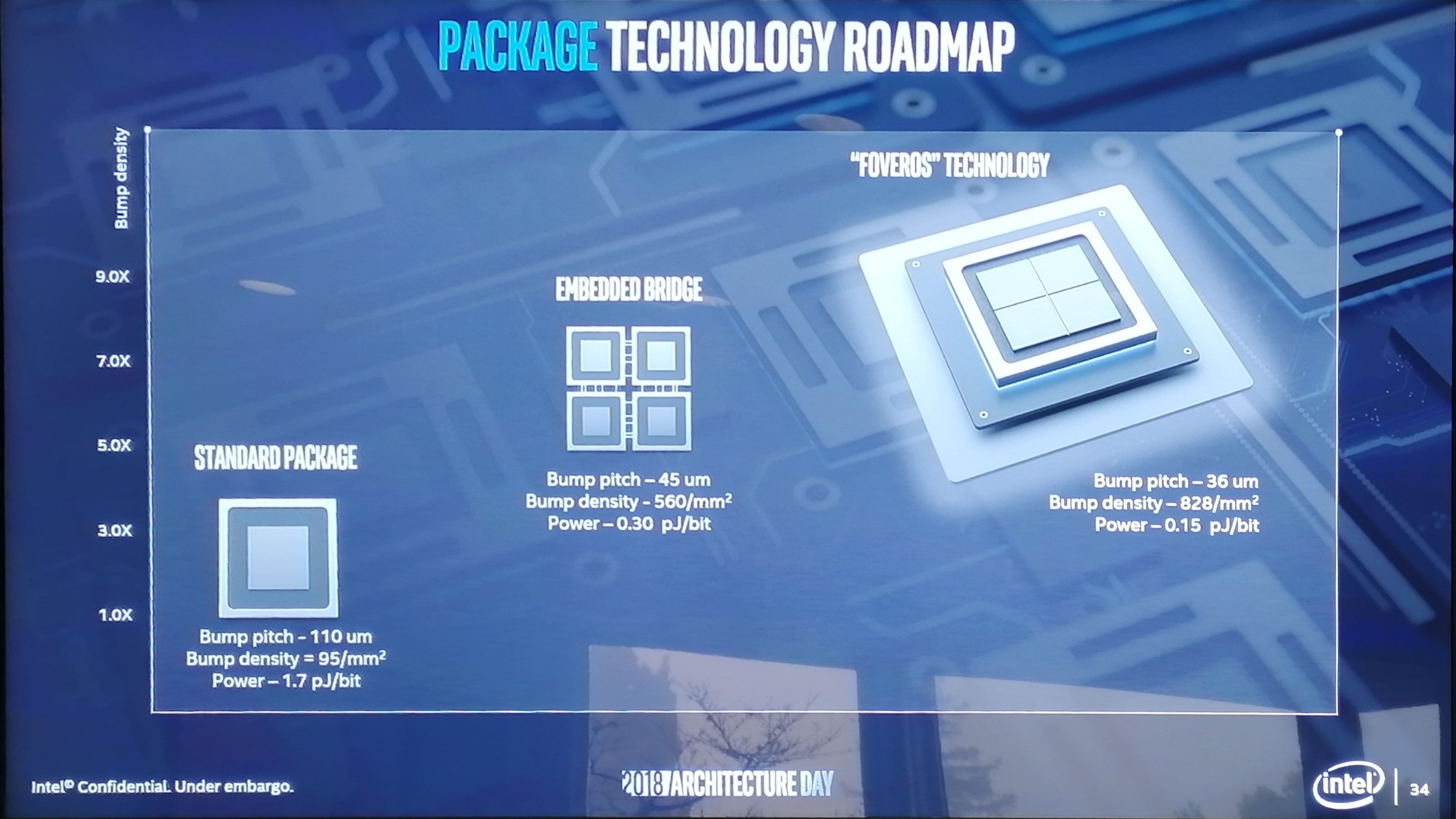
Q: In the demo of FOVEROS, the chip combined both big x86 cores built on the Core microarchitecture and the small x86 cores built on the Atom microarchitecture. Can we look forward to a future where the big and little cores have the same ISA?
R: We are working on that. Do they have to have the same ISA? Ronak and the team are looking at that. However I think our goal here is to keep the software as simple as possible for developers and customers. It's a challenge that our architects have taken up to ensure products like this enter the market smoothly. We’ll also have a packaging discussion next year on products like this. The chip you see today, while it was designed primarily for a particular customer to begin with, it’s not a custom product, and in that sense will be available to other OEMs.
M: We've made the first step on a journey. That first step is a leap, and the next step is incremental. As we've said about One API strategy – if we homogenise the API then it'll go into all our CPUs. FOVEROS is also a new part/product that shows that we had a gap in our portfolio – it has helped us create technologies to solve an issue and we expect to expand on this in the future with new IP.
Q: Are you having fun with FOVEROS?
J: Because Raja deals in GPUs, he’s having fun with high bandwidth communications between compute elements. It's a new technology and we're having some experimentation with it. What is frustrating is that as an industry we hit a limit for current flux density a year before stacking technology became viable, so for high performance on stacking we're trying a lot of things in different areas. There's no point having to make thermal setbacks if it also removes the reason why you're using the technology. But we're having fun and trying a lot, and we'll see FOVEROS in a number of parts over the next 5 years. We will find new solutions to problems we don't even know exist yet.
Q: When is Manufacturing Tech Day?
M: We will tell you when it happens! I'm sure you all have opinions on Intel 10nm right now and yes we are looking at what we're doing, eating an amount of humble pie, but we're re-adjusting our process to make sure that we can take the best process no matter what the product is.
The title of this page was a quote from Jim during the Q&A: 'At some point in the future you'll read an article with the title Intel Made Something Really Funny.'. I think I win this bet...


148 Comments
View All Comments
ajc9988 - Thursday, December 13, 2018 - link
https://www.anandtech.com/show/13445/tsmc-first-7n...Risk production is in Q2 next year. And Mass is listed by Q2 2020 for 5nm.
https://www.extremetech.com/mobile/278800-tsmc-exp...
So, I was a bit off by the estimate for volume being 2020, but you were off on when risk production starts. Meanwhile, 7nm+ is already confirmed for AMD on Zen3, as the benefits of 5nm+ don't outweigh the costs associated moving to the process for AMD. This is why it is thought AMD will skip 5nm and try 3nm when available. But, TSMC has not said when 3nm will be available, while Samsung is saying 3nm in 2021:
https://semiengineering.com/big-trouble-at-3nm/
https://www.cdrinfo.com/d7/content/samsung-details...
http://www.semimedia.cc/?p=2524 (saying TSMC 3nm in 2022/23)
I cannot find the article speculating Apple will be the first customer on 5nm EUV and when ATM.
HStewart - Thursday, December 13, 2018 - link
"Nodes are marketing jargon"Exactly - it reminds me the frequence wars back in P4 days. But if you look closely at Intel's plan - I am no chip designer - even though I did take Micro-code Enginnering classes in College, but Foveros is revolutionary design - I thought EMiB was amazing, but to do that in 3rd diminsion is awesome - maybe one they could even stack cores that way - instead huge chip monsters.
But a nm rating by vendor 1 does not nm rating by vendor 2 - what underneath makes the different - Intel is extremely smart to decouple nm process from actual archexture. If you notice by Intel archiexture Intel has more improvements in core archiexture over next 3 years - this is because they are not limited by process (nm)
ajc9988 - Friday, December 14, 2018 - link
EMIB was not revolutionary and neither is foveros. They are incremental steps and existing competing solutions are available and have been for some time. Not only that, it will only be used on select products with eventual spread to the stack.Go to the second page of comments and see my links there. I think you will find those quite interesting. Not only that, this has been done with HBM for years now. If you look at AMD's research, almost half a decade ago, they were studying optimal topologies for active interposers. They found only 1-10% of the area was needed for the logic routing of an active interposer. Moving a couple I/O items onto the active interposer just is an extension. In fact, you can put those components on a spread out interposer between the above chiplets that sit on the interposer, but would need to plan on the heat dissipation or having so low a heat that it doesn't need sinked.
Considering lack of details of what is on the active interposer or timeline for mainstream, HEDT, and server markets, I will assume those won't see this until 2020, with the first products being mobile in nature.
In fact, Intel this summer gave AIB patents to DARPA to try to control what tech is used for chiplets moving forward, proposing that be used. AMD proposed a routing logic protocol which would be agnostic to routing on the chiplets itself, increasing compatibility moving forward.
Now, if EMIB is so "revolutionary", do the Intel with AMD GPUs seem revolutionary? Because that is the only product that comes to mind that uses it. Those chips are Hyades Canyon and Crimson Canyon. It isn't that dissimilar to other data fabric uses.
So far, on disintegration of chip components, AMD's Epyc 2 is getting there. It literally uses just cores and the interconnect for the chiplet (for this description, I am including cache with the cores, but when latency is reduced with active interposers, I do expect an L3 or L4 or higher caches or integrated memory on package to be introduced external to the "core" chiplet moving forward). From there, we could see the I/O elements further subdivided, we could see GPU, modems, etc. But all of this has been planned since the 2000s, so I don't see anything new other than the culmination around the same time other alternative solutions are being offered, just that the cost/benefit analysis has not tipped in its favor just yet, but should in the next year or so, which should bring many more designs to the forefront. Here is a presentation slideshow discussing the state of current 2.5D and 3D packaging. After review, I'd like to hear if you still think EMIB and Foveros are "revolutionary." Don't get me wrong, they are an incremental success and should be honored as such. But revolutionary is too strong a word for incremental process. Overall, it changes nothing and is the culmination of a lot of work over a decade by numerous companies and engineers. Even competing solutions can act as inspiration for another company moving forward and Intel's engineers read the whitepapers and published peer reviewed articles on the cutting edge, just like everyone else in the industry.
As to you saying Intel is smart to do it, they haven't done it except in silicon in labs and in papers, unless talking the EMIB with Intel CPU. AMD has a product line, Epyc 2, where the I/O is made at GF on 14nm and the chiplet is made on 7nm TSMC with greater pitch disparity. Intel hasn't really removed the components off the core chip yet into each separate element. ARM is considering something similar, and this is the logical progression for the custom designed chips for RISC V moving forward (may take a little longer, less well funded).
Meanwhile, this doesn't seem to stack high performance cores on high performance cores. The problem of thermals cooking the chip are too great to solve at this moment, which is why low power components are being placed relative to the higher performance (read as higher heat producing) components. Nothing wrong with that, it makes sense.
But, what doesn't make sense is your flowering lavish praise on Intel for something that doesn't seem all that extraordinary in light of the industry as a whole.
johannesburgel - Thursday, December 13, 2018 - link
People keep saying the same thing about Intel's 14nm process, which is allegedly equal or better than other fab's 10nm processes. But AMD currently makes products on 14nm and 12 nm processes which Intel apparently can't build on its own 14nm process. For example there is still no 32-core Xeon while AMD will soon ship 64 core EPYCs and lots of other companies have 32/48/64 core designs on the market. Many Intel CPUs have much higher effective TDPs than their equivalent AMD CPUs.So pardon me if I am not willing to simply believe in all this "Intel's process is better in the end" talk.
HStewart - Thursday, December 13, 2018 - link
But intel's single core performance is better than AMD's single core performance. Just because AMD glues 8 core cpus together does not make them betterIcehawk - Thursday, December 13, 2018 - link
Node isn't even close to everything.Rudde - Wednesday, December 12, 2018 - link
Gen 11 graphics in desktops is said to reach double the performance of gen 9.5 desktop graphics. 2W Atoms have half the max frequency of desktop graphics and half or three quarters of the execution units. The 7W custom hybrid processor has the full amount of execution units. I'd guess it has half the frequency of it's desktop counterpart to stay within power limits. This would put it at the same performance as 9.5-gen desktop parts, or actually at 30% higher performance.Think about that. 80% single thread performance compared to current high-end desktop processors (my quick est.) and 130% graphics performance. That's a solid notebook for web browsing, legacy programs and even for light gaming. All that at a power budget of a tablet.
If I were to bet, I'd bet on a MS Surface Book.
Spunjji - Thursday, December 13, 2018 - link
Now that would be nice!Intel999 - Wednesday, December 12, 2018 - link
Keep in mind that 3DXpoint came to market three years past the initial promise from Intel. 10nm will be appearing 4 or 5 years late depending on when volume production materializes.Chances are that this 3D stacked promise for late 2019 will show up around 2022.
I'm seeing alot of fellow Intel fanboys show a semblance of confidence that has been absent in recent months and rightfully so.
Let's all hope Intel can deliver this time on time.
ajc9988 - Wednesday, December 12, 2018 - link
I disagree on worrying about Intel with the active interposer. They use passive interposers for the mesh on HEDT and Xeons and Xeon Phi (since around 2014) for years now. The 22nm active interposer is to fill out fab time due to pushing chipsets back to plants that were going to be shut down due to moving to 10nm, which never came.Meanwhile, AMD did a 2017 cost analysis saying that below 32nm would cost as much as a monolithic die, so it seems they are waiting due to cost, not on technical capability.
Either way, Intel doesn't hit 7nm until 2021, around the time 3nm may be ready at TSMC, if they go to 3nm within a year of volume 5nm products expected in 2020. That means Intel will never regain the process lead moving forward in any significant way, unless everyone else gets stuck on cobalt integration.