NVIDIA GeForce 6800 Ultra: The Next Step Forward
by Derek Wilson on April 14, 2004 8:42 AM EST- Posted in
- GPUs
NV40 Under the Microscope
The NV40 chip itself is massive. Weighing in at a hefty 222 Million transistors, NVIDIA's newest GPU has more than three times the number of transistors as Intel's Northwood P4, and about 33% more transistors than the Pentium 4 EE. This die is droped onto a 40mm x 40mm flipchip BGA package.
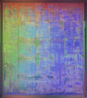
NVIDIA doesn't publish their die size information, but we have been able to interpolate a little bit from the data we have available on their process information, and a very useful wafer shot.
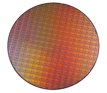
As we can see, somewhere around 16 chips fit horizontally on the wafer, while they can squeeze in about 18 chips vertically. We know that NVIDIA uses a 130nm IBM process on 300mm wafers. We also know that the P4 EE is in the neighborhood of 250mm^2 in size. Doing the math indicates that the NV40 GPU is somewhere between 270mm^2 and 305mm^2. It is difficult to get a closer estimate because we don't know how much space is between each chip on the wafer (which also makes it hard to estimate waste per wafer).
Since we don't have information on yields either, it's hard to say how well NVIDIA will be making out on this GPU. Increasing the transistor count and die size will lower yields, and the retail value of cards based on NV40 will have the same price at release as when NV38 was released.
Of course, even if they don't end up making as much money as they want off of this card, throwing down the gauntlet and pushing everything as hard as they can will be worth it. After the GeForce FX series of cards failed to measure up to the hype (and the competition), NVIDIA has needed something to reestablish their position as performance leader in the industry. This industry can be brutal, and falling short twice is well nigh a death sentence.
But, all those transistors on such a big die must draw a lot of power right? Just how much juice do we need to feed this beast ...


77 Comments
View All Comments
TheAudit - Wednesday, April 14, 2004 - link
Nice!MemberSince97 - Wednesday, April 14, 2004 - link
You guys shoulda done a mini review of that 510W PSU that was used....Verdant - Wednesday, April 14, 2004 - link
looks awesome congrats to nvidia on raising the bar!personally i don't game very much, and the only reason my Geforce2 was replaced was for the dual-heads of the Radeon 9000
but as an enthusiast, any leaps make me excited :p
can't want to see ATIs new cards
Lonyo - Wednesday, April 14, 2004 - link
Not as impressive as other sites made it look in many circumstances.But still quite boost in performance.
NYHoustonman - Wednesday, April 14, 2004 - link
Jesus... Ya, looks like I'll be upgrading before college...gordon151 - Wednesday, April 14, 2004 - link
Damn, two independant cable lines and a 480W PSU. Good thing it kills in performance, but still too pricey for me. Bring on the 6800XT for us broke people :P.KristopherKubicki - Wednesday, April 14, 2004 - link
Impressive green one.Hope it doesnt cost $500.
Kristopher