The Samsung Galaxy S9 and S9+ Review: Exynos and Snapdragon at 960fps
by Andrei Frumusanu on March 26, 2018 10:00 AM ESTThe Exynos 9810 - Introducing Meerkat
The Exynos 9810 made a lot of noise this year as S.LSI made astounding claims of up to 2x better single-threaded performance and a 40% uplift in multi-threaded performance. We exclusively covered the first public disclosure of the microarchitecture later in January and showed that Samsung’s performance claims were not farfetched at all. Before we got back to the CPU core, let’s see what else the Exynos 9810 brings to the table.
| Samsung Exynos SoCs Specifications | ||
| SoC | Exynos 9810 | Exynos 8895 |
| CPU | 4x Exynos M3 1c@2.7, 2c@2.3, 3-4c@1.79 GHz 4x 512KB L2 4096KB L3 4x Cortex-A55 @ 1.79 GHz No L2 512KB L3 |
4x Exynos M2 @ 2.314 GHz 2048KB L2 4x Cortex-A53 @ 1.690GHz 512KB L2 |
| GPU | Mali G72MP18 | Mali G71MP20 @ 546MHz |
| Memory Controller |
4x 16-bit CH LPDDR4x @ 1794MHz |
4x 16-bit CH LPDDR4x @ 1794MHz 28.7GB/s B/W |
| Media | 10bit 4K120 encode & decode H.265/HEVC, H.264, VP9 |
4K120 encode & decode H.265/HEVC, H.264, VP9 |
| Modem | Shannon Integrated LTE (Category 18/13) DL = 1200 Mbps 6x20MHz CA, 256-QAM UL = 200 Mbps 2x20MHz CA, 256-QAM |
Shannon 355 Integrated LTE (Category 16/13) DL = 1050 Mbps 5x20MHz CA, 256-QAM UL = 150 Mbps 2x20MHz CA, 64-QAM |
| ISP | Rear: 24MP Front: 24MP Dual: 16MP+16MP |
Rear: 28MP Front: 28MP |
| Mfc. Process |
Samsung 10nm LPP |
Samsung 10nm LPE |
At the heart of the Exynos 9810 we see four Exynos M3 CPU cores, which run at thread-count dependent maximum frequency. This ranges from up to 2.7GHz in single-threaded scenarios, to 2.3GHz in dual-core mode, and 1.79GHz in full quad-core mode.
Alongside the big performance CPUs we also see Samsung’s introduction of Cortex-A55 cores in a quad-core configuration running at up to 1.79GHz (down from the MWC units, which were running at up to 1.9GHz). The interesting thing to note is that unlike the Snapdragon 845, the A55 cores in the Exynos are in their own cluster and not shared with the M3’s.
The GPU is a new Mali G72MP18 running at up to 572MHz. The GPU configuration was a surprise here as not only did Samsung opt to go for a smaller configuration than last year’s MP20, but the clock frequency also hasn’t increased much from the Exynos 8895’s 546MHz.
On paper, the Exynos 9810 has a stronger modem than the Snapdragon 845 as it supports up to 6x carrier aggregation vs the S845’s 5xCA. The upload streams also support 256-QAM which allows for 33% higher upload speeds compared to the Exynos 8895 and Snapdragon’s modems.
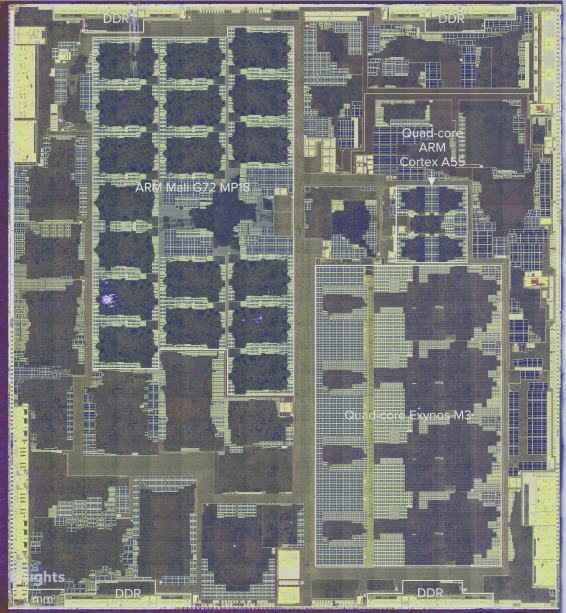
Exynos 9810 Floor Plan. Image Credit TechInsights
TechInsights really delighted us this time around as they also released a die shot of the Exynos 9810 last week. The 9810 comes in at 118.94mm², which is 14% bigger than the 8895’s 103.64mm². Qualcomm seems to have an edge in total die size and we don’t have to look very closely to notice why.
At 20.23mm² the Exynos M3 complex is absolutely massive compared to other mobile SoC CPUs. At 3.46mm² for the core and accompanying L2 the Meerkat core is over twice as big as the 1.57mm² of the A75+L2 in the Snapdragon 845, granted that the latter has half the L2 cache. Meerkat indeed almost matches Apple’s Monsoon cores in the A11 which come in at 2.68mm² - but only if one takes into account the L2 cache of the M3 for which I roughly estimate 0.88mm². Apple also has a slight density advantage due to TSMC’s 10FF manufacturing node.
Nevertheless, at a total of 22.1mm² for both clusters Samsung has thrown down a lot of silicon for the CPU complexes, far more than Apple’s 14.48mm² and Qualcomm’s 11.39mm².
An interesting aspect we can see in the die shot is the way that Samsung arranges the L3. Indeed we reached out again to ARM for clarification on if the DSU allows third-party cores to be used, and contrary to we had been told last year, ARM doesn’t enable third-party cores to be connected. This means that the L3 we see here on the M3’s are of Samsung’s own design. At 4MB, the cache is quite big, but as mentioned, the layout is unlike anything we’ve seen before as it looks like not only does Samsung distribute the L3 SRAM banks in a row/column, but the L3 arbitration logic and L3 tags are also distributed among the banks alongside each M3 core.
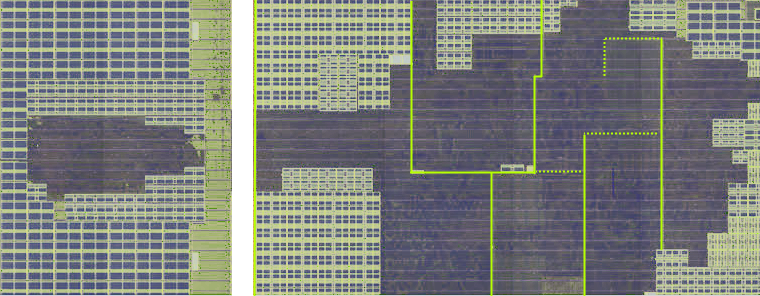 Image Credit TechInsights
Looking closer at the core we see two L2 banks (512KB total) along with their tag buffers on the left side. At the top middle we see what is likely the 64KB L1D cache with the load/store engine. On the right side, likely on the bottom, we see the L1I cache as well as other front-end related memories. Unfortunately Samsung’s physical implementation here is a sea of gates and it’s hard to make out the individual CPU engines.
The Cortex-A55 cluster looks quite similar to the Exynos 8895’s A53 cluster – this is due to the lack of per-core L2’s and only a shared 512KB L3 that essentially acts as a shared L2. The performance degradation of the A55s not having L2’s is offset somewhat by the fact that the L3 is run at the same frequencies as the cores – eliminating the need for asynchronous bridges between the cores and the cache and thus reducing the L3 cache latency compared to a normal DSU configuration.
Finally the last interesting take-away from the die shot is the GPU. The Mali G72MP18 comes in at a total of 24.53mm² which is smaller than last year’s >~32mm² behemoth based on the Mali G71MP20. Here it’s clear just much of an advantage Qualcomm has as the Adreno 630 with its 10.69mm² is outright tiny compared to the Mali and even has a significant lead even over Apple’s A11 GPU which comes at 15.28mm².
2.9GHz.. 2.7GHz .. 2.3GHz ... 1.79GHz?? Which is it?
One of the bigger discussion points about the Exynos 9810 was its clock frequency. Samsung had initially announced a peak clock frequency of 2.9GHz but immediately that seemed unlikely given S.LSI’s history of backing down on their initial frequency claims.
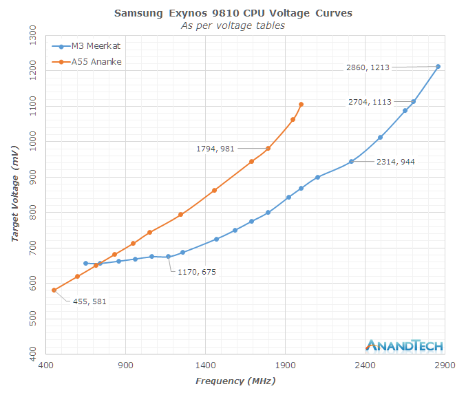
Looking at the voltage tables of the Exynos 9810 points out quite a wide range of voltages for the M3 cores, but it’s the far end that seems quite problematic. To actually reach the initially advertised state of 2.9GHz (2860MHz), it takes an extremely high voltage of 1213mV. Backing down to 2704MHz with which the Galaxy S9 is released ends up with an already drastic decrease of 100mV. Historically Samsung has always had quite high voltages at the far end of the frequency tables as it seems they optimise the physical implementation for leakage and power, which in turn requires higher voltages to reach high frequencies.
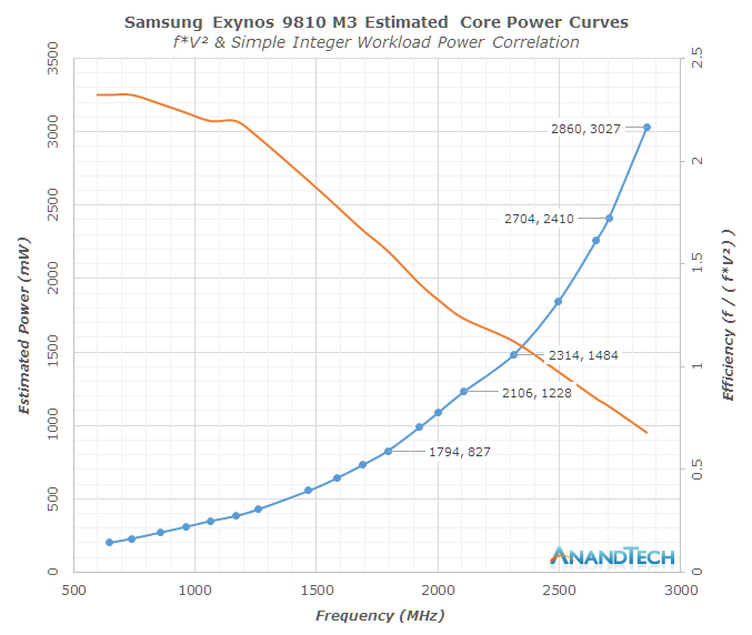
When looking at the power curves correlated with our traditional integer power virus we see that there’s an immense increase in power consumption at the higher frequencies. Indeed going from 2.3GHz to 2.9GHz would have doubled power usage, and even 2.7GHz comes at a steep power price. Given that power usage scales roughly along the lines of voltage cubed, the SoC's efficiency suffers with the increased frequency. The good news here is that Samsung’s efficiency curve is quite steep and linear, that means backing down on frequency should see significant efficiency gains.
Samsung’s decision to limit 2+ core frequencies makes sense in the context of thermal constraints. Even if a CPU core is very efficient at its peak performance, it’s just physically not possible to run multiple cores at peak performance as the SoC just lacks the required thermal dissipation. It’s also important to emphasise this difference between power usage and efficiency: This is no Snapdragon 810 situation where we have high power but with lacking performance. Total energy usage of the M3 should thus be equal to a lower performance core which uses less power.
The only comment I’d like to add here is that I think Samsung would have done a lot better if the M3 cores had been split into a 2+2 configuration with separate frequency and voltage planes. This is something we'll get back to in the battery life section of the review.
I’ve had a look through Samsung’s scheduler and DVFS mechanisms which controls the switching between the 1/2/3/4 core modes and generally I’ve been unimpressed by the implementation. Samsung had made use of hot-plugging to force thread migrations between the cores which is an inefficient way of implementing the required mechanism. The scheduler is also tuned extremely conservatively when it comes to scaling up performance, also something we’ll see the effects of in the system performance benchmarks.
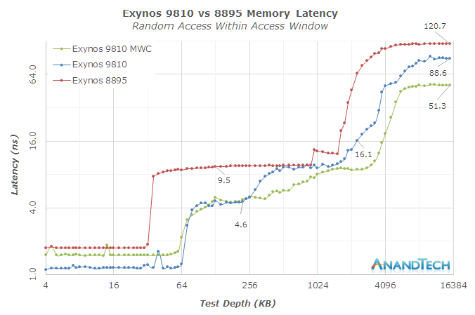
Lastly, I noticed that the commercial unit we acquired had quite different DVFS settings that I was unable to reproduce the excellent memory latency scores I had measured on the launch event devices at MWC. This means that the memory performance is going to be less than I had anticipated, and metrics such as full random access latency actually saw a degradation compared to the Exynos 8895.


190 Comments
View All Comments
id4andrei - Tuesday, March 27, 2018 - link
All reviewers go gaga for geekbench scores with iphones/ipads as well. In this case the GB scores prove that at least in chip design Samsung has made a huge leap. As the review has outlined, the problem lies with the scheduler and DVFS which Samsung can and should address.If "Samdung" is so bad at hardware design, how do you call Apple's high priced iphones of the last 3 years that could not sustain chip performance and had to be throttled so as to not crap out. All initial reviews were glowing but they were all impervious to the impeding throttling.
name99 - Tuesday, March 27, 2018 - link
Dude, you really do yourself no favors by struggling so hard to criticize Apple.Apple's throttling has NOTHING to do with the CPU per se (ie the CPU is not generating excessive heat beyond spec, or because it has been running too fast for too long), it has to do with the BATTERY and with a concern that, if CPU performance were to spike the battery could not supply enough current.
Very different problem, nothing to do with the CPU design. A real problem yes but totally irrelevant to the issues being discussed here.
Matt Humrick - Wednesday, March 28, 2018 - link
Apple's big CPU and GPU are susceptible to thermal throttling when running sustained workloads too.Also, having to throttle a processor within a year of sale because its transient current requirements overwhelm the power delivery system is most definitely a design flaw.
Icehawk - Friday, April 6, 2018 - link
My wife’s 6S is still working at 100% after several years, I get the feeling the amount of people affected is overblown as pretty much anything anti-Apple is. I do think Apple needs to look at a better way of dealing with this but it’s also not the armeggedon somemake it out to be. I am far from a Apple fanboy but I do like their iOS products but I am sure someone will make a retort of that nature. I’d say the same thing about the Samsung chip - not great but it is performant, perhaps if we stop thinking each year a new phone should blow us away it would help us be more realistic.Lavkesh - Tuesday, March 27, 2018 - link
"In this case the GB scores prove that at least in chip design Samsung has made a huge leap" - Please explain huge leap here? The new chip barely outperforms the older SOC.ZolaIII - Monday, March 26, 2018 - link
I am very disappointed with both SoC's. Qualcomm wasted so much space on bad L4 cache which only added to latency & generally wasted more. The 30% is enormous even if new A75 cores are 35% bigger (would be 50% with ARM's L2 reference cache size) I don't know about A630 vs A540 size but if it grown-up let's say 10% the cores & GPU would together accommodate for around 15~20% leaving L3 & L4 responsible for the rest. Would be much better they used it for GPU as it could had been 2x the size then. I am also very disappointed with new cache hierarchy as it turns out to be stupid and a waist of silicone. Seams to me neither SoC used good scheduler nor scheduling by the looks of things it seems Samsung used the CAF HPM sched settings for Snapdragon SoC very aggressive patched interactive without any restraints whatsoever & no hotplug whatsoever which is very south from optimal, reference QC platform seams to had at least used hotplug (as their is no other way to explain the difference of almost 1W in GPU testing as two vs four A75's active). On the other hand seems Samsung used Power aware schaduler instead HPM & very granulated hotplug producing very bad results as those are directly confronted two things & when splashed together can only result in catastrophic result. I prefer HPM configured to be used with limited task packing and a high priority tasks enabled with significant increase of time interval for it (so that it can skip CPU sched limit), for CPU sched interactive traditional not patched with tree step load limitations (idle so that it doesn't jump erratic on any back shade task, ideal that is considered as best sustainable leakage for given lithography & max sustainable for two core's [only on big cores] i also use boost enabled & set to ideal frequency one [same as in interactive]). Preferred to use core_ctl hotplug disabled for the two little & two big cores so that they never get switched off from it. I won't go further in details about it hire as its pointless. I find this idea balanced between always available/needed/total performance as most of the times two of each course are enough for most of tasks & if not it's not a biggie to wait for other two to kick in. There is a minor drow back in responsiveness on lite task's but actually it works as fast as possible on hard one's flagged as heavy tasks like for instance Chrome rendering. It's also very beneficial to GPU workloads where even switching of two little core's and giving even 100~150mv headroom to GPU means much.Sorry for getting a bit deep regarding how complete scheduling mechanism should be done but I had an urge to explain how it should be done as it's so terrible done in the both cases examined hire.
tuxRoller - Wednesday, March 28, 2018 - link
It's not at all clear that the hpm is meaningfully better (much faster or much more power efficient) than a proper schedtune + energy model implementation.Scheduling is just ridiculously hard. Adding the constraints of: soft-realtime requirements, minimal battery usage, AND an asmp and you've got the current situation where there's not yet a consensus design. We are, however, starting to see signs of convergence, imho.
zeeBomb - Monday, March 26, 2018 - link
I came...and I finally sawphoenix_rizzen - Monday, March 26, 2018 - link
Ouch. The Exynos S9 is just barely better than the Exynos S7. :( And that's what Canada's going to get.Here's hoping they can improve things via software updates. Was considering the S9 to replace the wife's now dead S6. She's been using my S7 for the past two months while I limp along with a cracked-screen Note4. Other than the camera and screen, this isn't looking like much or an upgrade for being two generations newer.
Maybe we'll give the ZTE, Huawei, and Xiaomi phones another look ...
mlauzon76 - Monday, March 26, 2018 - link
Samsung Exynos 9810 (Europe & Rest of World)Canada is the 'rest of [the] world', but we don't get that version, we never get anything with the Exynos processor, we get the following one:
Qualcomm Snapdragon 845 (US, China, Japan)