The AMD Ryzen Threadripper 1950X and 1920X Review: CPUs on Steroids
by Ian Cutress on August 10, 2017 9:00 AM ESTSilicon, Glue, & NUMA Too
In the Ryzen family, AMD designed an 8 core silicon die known as a Zeppelin die. This consisted of two core complexes (CCX) of four cores each, with each CCX having access to 8 MB of L3 cache. The Zeppelin die had access to two DRAM channels, and was fixed with 16 PCIe lanes for add-in cards. With Threadripper, AMD has doubled up the silicon.
If you were to delid a Threadripper CPU, you would actually see four silicon dies, similar to what an EPYC processor would have, making Threadripper a Multi Core Module (MCM) design. Two of these are reinforcing spacers – empty silicon with no use other than to help distribute the weight of the cooler and assist in cooling. The other two dies (in opposite corners for thermal performance and routing) are basically the same Zeppelin dies as Ryzen, containing eight cores each and having access to two memory channels each. They communicate through Infinity Fabric, which AMD lists as 102 GB/s die-to-die bandwidth (full duplex bidirectional), along with 78ns to reach the near memory (DRAM connected to the same die) and 133ns to reach the far memory (DRAM on another die). We confirmed those numbers on DDR4-2400 memory, also achieving 65 ns and 108 ns respectively using DDR4-3200.
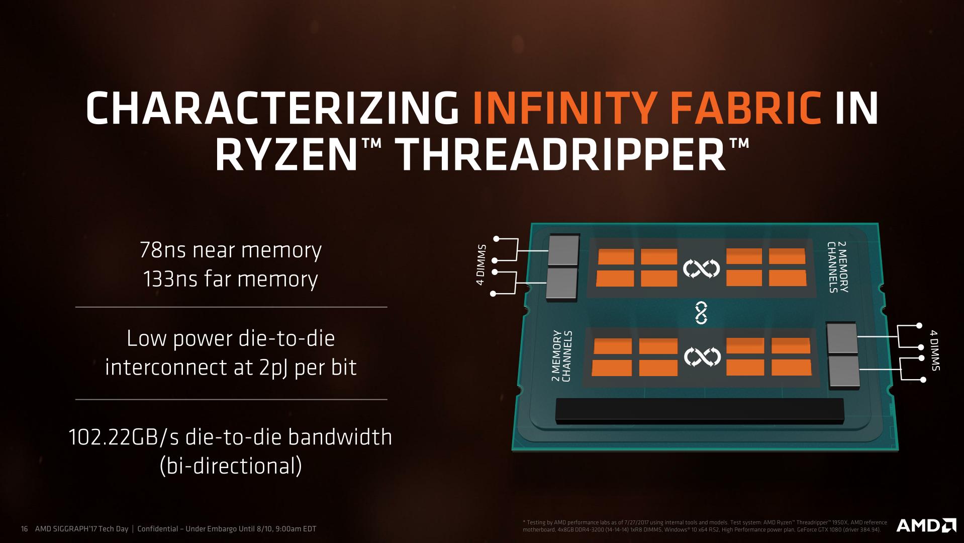
Despite this AMD slide showing two silicon dies, there are four units of silicon in the package. Only two of the dies are active, so AMD has 'simplified' the diagram'
By comparison, EPYC lists die-to-die bandwidth as 42.6 GB/s at DDR4-2666. This is because EPYC runs fabric links to three dies internally and one die externally (on the next socket), which maximizes all the links available. The dies in Threadripper only have to communicate with one other die, so has more flexibility. To that extent, we’re under the impression that Threadripper is using two of these links at 10.4 GT/s using the following method:
- Die to Die for EPYC is quoted as 42.6 GB/s at DDR4-2667
- Die to Die for Threadripper is quoted as 102.2 GB/s at DDR4-3200
- 42.6 GB/s * 2 links * 3200/2667 = 102.2 GB/s
- 42.6 GB/s * 3 links * 3200/2667 at 8.0 GT/s = 115.8 GB/s (too high)
- 42.6 GB/s * 3 links * 3200/2667 at 6.4 GT/s = 92.6 GB/s (too low)
This configuration for AMD is essentially what the industry calls a NUMA configuration: non-uniform memory access. If left as it, it means that code cannot rely on a regular (and low) latency between requesting something from DRAM and receiving it. This can be an issue for high-performance code, which is why some software is designed NUMA-aware, so that it can intelligently pin the memory it needs to the closest DRAM controller, lowering potential bandwidth but prioritizing latency.
NUMA is nothing new in the x86 space. Once CPUs began shipping with on-die memory controllers rather than using an off-die memory controller in the Northbridge, NUMA became an inherent part of multi-socket systems. In this respect AMD was the leader here right from the start, as they beat Intel to on-die memory controllers for x86 CPUs by years. So AMD has been working with NUMA for years, and similarly NUMA has been the state of affairs for Intel's multi-socket server systems for almost a decade.
What's new with Threadripper however is that NUMA has never been a consumer concern. MCM consumer CPUs have been few and far between, and we'd have to go all the way back to the Core 2 Quad family to find a CPU with cores on multiple dies, which was a design that predates on-die memory controllers for Intel. So with Threadripper, this is the very first time that consumers – even high-end consumers – have been exposed to NUMA.
But more importantly, consumer software has been similarly unexposed to NUMA, so almost no software is able to take its idiosyncrasies into account. The good news is that while NUMA changes the rules of the game a bit, it doesn't break software. NUMA-aware OSes do the heavy lifting here, helping unaware software by keeping threads and memory accesses together on the same NUMA node in order to ensure classic performance characteristics. The downside to this is that much like an overprotective parent, the OS is going discourage unaware software from using other NUMA nodes. Or in the case of Threadripper, discouraging applications from using the other die and its 8 cores.
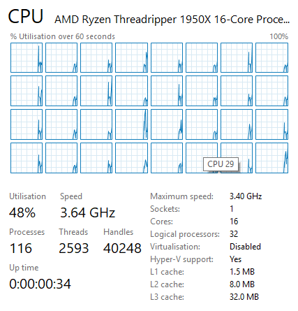
At a hardware level, Threadripper is natively two NUMA nodes
In an ideal world, all software would be NUMA-aware, eliminating any concerns over the matter. From a practical perspective however, software is slow to change and it seems unlikely that NUMA-style CPUs are going to become common in the future. Furthermore NUMA can be tricky to program for, especially in the case of workloads/algorithms that inherently struggle with "far" cores and memory. So the quirks of NUMA are never going to completely go away, and instead AMD has taken it upon themselves to manage the matter.
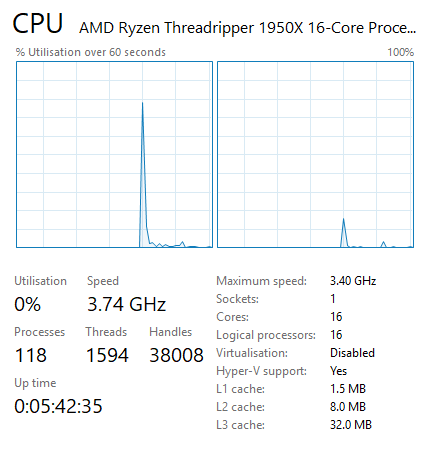
AMD has implemented BIOS switches and software switches in order to better support and control the NUMAness of Threadripper. By default, Threadripper actually hides its NUMA architecture. AMD instead runs Threadripper in a UMA configuration: a uniform memory access system where memory is sent to any DRAM and the return is variable in latency (e.g. ~100ns averaging between 78ns and 133ns) but focusing for a high peak bandwidth. By presenting the CPU to the OS as a monolithic, single-domain design, memory bandwidth is maximized and all applications (NUMA-aware and not) see all 16 cores as part of the same CPU. So for applications that are not NUMA-aware – and consequently would have been discouraged by the OS in NUMA mode – this maximizes the number of cores/threads they can use and the memory bandwidth they can use.
All 32 threads are exposed as part of a single monolithic CPU
The drawback to UMA mode is that because it's hiding how Threadripper really works, it doesn't allow the OS and applications to make fully informed decisions for themselves, and consequently they may not make the best decisions. Latency-sensitive NUMA-unaware applications that fare poorly with high core/memory latencies can struggle here if they use cores and memory attached to the other die. Which is why AMD also allows Threadripper to be configured for NUMA mode, exposing its full design to the OS and resulting in separate NUMA domains for the two dies. This informs the OS to keep applications pinned to one die when possible as previously discussed, and this mode is vital for some software and some games, and we’ve tested it in this review.
Overall, using a multi-silicon design has positives and negatives. The negatives end up being variable memory latency, variable core-to-core latency, and often redundancy in on-die units that don’t need to be repeated. As a result, AMD uses 400mm2+ of silicon to achieve this, which can increase costs at the manufacturing level. By contrast, the positives are in silicon design and overall yeilds: being able to design a single piece of silicon and repeat it, rather than design several different floor plans which multiplies up the design costs, and having the (largely) fixed number of wafer defects spread out over many more smaller dies.
By contrast, Intel uses a single monolithic die for its Skylake-X processors: the LCC die up to 10-core and HCC die from 12-core up to 18-core. These use a rectangular grid of cores (3x4 and 5x4 respectively), with two of the segments reserved for the memory controllers. In order to communicate between the cores, Intel uses a networking mesh, which determines which direction the data needs to travel (up, down, left, right, or accepted into the core). We covered Intel’s MOdular Decoupled Crossbar (MoDe-X) methodology in our Skylake-X review, but the underlying concept is consistency. This mesh runs at 2.4 GHz nominally. Prior to Skylake-X, Intel implemented a ring topology, such that data would have to travel around the ring of cores to get to where it needed to go.
With reference to glue, or glue-logic, we’re referring to the fabric of each processor. For AMD that’s the Infinity Fabric, which has to travel within the silicon die or out to the other silicon die, and for Intel that’s the internal MoDe-X mesh. Elmer’s never looked so complicated.


347 Comments
View All Comments
Lolimaster - Friday, August 11, 2017 - link
Adding useless singe thread benchs for people that will pay $600+ for many cores is plain stupidity like that useless open a pdf test.casperes1996 - Saturday, August 12, 2017 - link
Why do you bother replying to these, Ian? I love your enthusiasm about what you do, and am happy that you reply to comments, but as you state yourself, no matter what you say, you'll be called a shill on more than a weekly basis by either side no matter what you do. Intel shill, AMD shill, Apple shill, Nvidia shill and so on. There's no stopping it, because you just can't please the people who go into something wanting a specific result. Well, you can if you give them that result, but sometimes, facts aren't what you want them to be, and some people don't accept that.Cheers, mate
Diji1 - Thursday, August 10, 2017 - link
You sound like a crazy person.Notmyusualid - Saturday, August 12, 2017 - link
@ Diji1You are correct.
He is implying just because we want HEDT platforms / chips, that we care nothing for single-threaded performance.
He is a true AMD fan-boi, as you will see over time.
lordken - Thursday, August 10, 2017 - link
@Johan Steyn: while I agree with you that the Intel piece with PR slide at the top was a little bit lame, I even lolled at "most scalable" part (isn't something like "glued" zen the most scalable design?) I think this review is good and goes also around architecture etc., there were few instances during reading when it seemed odd wording or being unnecessarily polite toward intel's shortcoming/deficit but I cant even remember them now.Though I was surprised about power numbers, as Toms measured much higher W for 7900X , 160-200 and with TTF even up to 250-331 , but here 7800/7900x had only ~150W.
Also this sentence is odd
"All the Threadripper CPUs hit around 177W, just under the 180W TDP, while the Skylake-X CPUs move to their 140W TDP." move to their? They are above the TDP...why not state it clearly?
tamalero - Thursday, August 10, 2017 - link
Im sratching my head on power consumption as well. Almost all reviewers shows that the i9's consume more than threadripper.Could be the motherboard used?
Some used the Zenith and other reviewers used the ASROCK retail one.
smilingcrow - Thursday, August 10, 2017 - link
Power consumption can vary a lot depending on the type of task and the exact nature of that task.So you should expect a lot of variation across reviews.
Johan Steyn - Thursday, August 10, 2017 - link
The amount of tests on games in this review is unbalanced. Also read my reply to Ian.Extremely well stated: " unnecessarily polite toward Intel's shortcoming" Sometimes I think these guys think all are complete mindless drones.
carewolf - Thursday, August 10, 2017 - link
It has always been like this here. This was pretty neutral by Anandtech standards, they even admitted it when it was faster.Johan Steyn - Thursday, August 10, 2017 - link
Please read my response to Ian, I think you are not looking close enough to what is happening here.