The Intel Skylake-X Review: Core i9 7900X, i7 7820X and i7 7800X Tested
by Ian Cutress on June 19, 2017 9:01 AM ESTDie Size Estimates and Arrangements
On the previous page, we showed pictures of ring bus and mesh arrangements. With a ring bus, ultimately the silicon layout of the cores and the interconnects can be regular but are not that stringent. Put the cores in a circle (or overlapping circles) and away you go. With a mesh, things get a little more rigid.
The mesh diagrams on the previous page are all presented as rectangles in x*y arrangements. You either have to add a full row or a full column to increase the die count, whereas in a ring it could be straight forward just to add another pair of cores into the ring (which is what happened over the last few generations). Adding a pair of cores in a mesh means that you end up with more corners and more edges – not all cores end up ‘equal’ and there can be performance penalties therein. Ideally, an arrangement where x = y is usually the best bet. This lets us make some predictions about how Intel’s silicon is lining up.
A side-note for discussion. If we had a 100x100 core arrangement, the cores in the middle would have big latency to get anywhere near external memory. Also, a 2D mesh could become a 3D mesh.
Three things come to our aid in discussing the LCC and HCC silicon. First was the original Skylake-X announcement back at Computex: one of Intel’s slides had an image of the basic floorplan of the HCC silicon to be used for the high core-count Skylake-X processors:
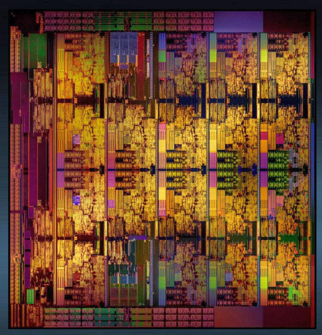
At the time, we were a bit stumped by this image. By counting the regular structures, we can see 4x5 arrangement, or rather a 20-core chip. On closer inspection two of the cores were different: on the second column, the top and bottom ‘cores’ did not look like cores. At the time we postulated that given the size of AVX512, this might be where they were. But the second piece of information was given through Intel’s mesh announcement.
Here’s the diagram:

This is meant to be a pseudo mockup of a theoretical core of n processors using the mesh topology. At the top are the socket links, along with the PCIe root complexes. However on the left and right are the DRAM controllers, essentially taking up the same area as a core but also using one of the mesh networking links.
So scoot back to that HCC die image, and zoom in on one of those odd looking ‘cores’:
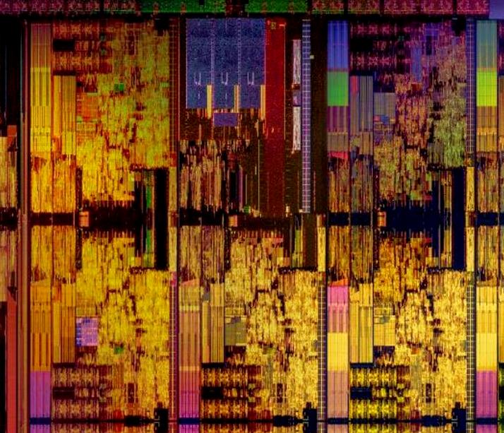
What we can see is three regular blue/green vertical areas, which means three on each side, for a total of six. Skylake-X only has four memory channels, but leaks have shown that the new Skylake-SP processors have six memory channels by design, so here they are. In the 4x5 grid, we have 18 cores and two sets of memory channels.
Back when Skylake-X was announced at Computex, I wrote that we were expecting the LCC silicon to be a 12-core design. At this time, we were still expecting Intel to use a ring-bus topology, and I mentioned before, adding two cores to a ring bus is fairly easy at the expense of peak latency between cores. Now that we know that Intel is using a mesh, it is quite different.
12 cores could quite easily fit into LCC silicon in a 3x4 arrangement, but that does not leave any room for the six memory controllers that the enterprise Xeons are all meant to have. If we added two ‘extra’ core sized areas for the 12-core design, we need a total of 14 segments. Using the x*y arrangement as required above, the only way 14 cores works is using a 7*2 arrangement. If this was the case, the DRAM controllers would essentially fill a whole row, or be at opposite ends of the column. If one of the x*y numbers is the number two, it makes more sense to use a ring bus any day of the week for power, die area and simplicity.
So that means that the 12-core SKU, the Core i9-7920X, is likely derived from the HCC 18-core silicon. Which also explains why that CPU has been delayed until August.
Die Sizes
At this point in time, the Skylake-X processors based on the LCC silicon have been in the hands of a few people. At Computex there were several extreme overclocking (using sub-zero coolants) events dedicated to the new processors. One element of recent extreme overclocking is delidding the processor and removing the integrated heat spreader to replace the thermal interface material underneath.
In general removing the IHS is not recommended without practice and experience, but for some processors in the past we have seen sizeable temperature benefits by replacing the standard thermal interface material (TIM) that Intel uses. The discussion on whether Intel should be offering a standard goopy TIM or the indium-tin solder that they used to (and AMD uses) is one I’ve run on AnandTech before, but there’s a really good guide from Roman Hartung, who overclocks by the name der8auer. I’m trying to get him to agree to post it on AnandTech with SKL-X updates so we can discuss it here, but it really is some nice research. You can find the guide over at http://overclocking.guide.
However removing the IHS means we can measure the silicon die.
The 10-core LCC die, which is a 3x4 design, measures in at 14.3 x 22.4, or 322mm2.
Using this, working from Intel’s 4x5 HCC diagram (and assuming it hasn’t been stretched), we can get 21.6 x 22.4 = 484mm2 for the high-core count design.
That leaves the Extreme core count option. Using the x*y strategy again, Intel could either run a 5x5 design, which gives 25 areas and 23 cores – which is unlikely. Next up is a 5x6 design, which gives 30 areas and 28 cores. It’s no secret that many leaks are pointing to a 28-core XCC processor at this point.
There’s also the fact that Intel provided this die shot at the Intel Manufacturing Day a few weeks ago, clearly showing the 5x6 arrangement:
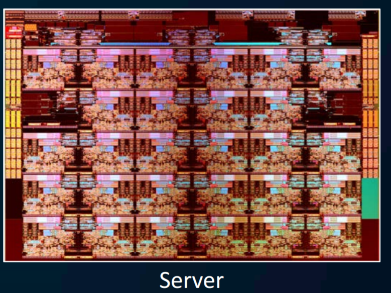
Doing the basic math on a 5x6 design gives us a 21.6 x 32.3 = 698mm2 die size for XCC.
| Skylake-SP Die Sizes | |||
| Arrangement | Dimensions (mm) |
Die Area (mm2) |
|
| LCC | 3x4 (10-core) | 14.3 x 22.4 | 322 mm2 |
| HCC | 4x5 (18-core) | 21.6 x 22.4 | 484 mm2 |
| XCC | 5x6 (28-core) | 21.6 x 32.3 | 698 mm2 |
Compared to other chips with Intel’s mesh architecture, Knights Landing comes in at 646mm2 (minus MCDRAM), and sources put Knights Corner at 720mm2.


264 Comments
View All Comments
mat9v - Tuesday, June 20, 2017 - link
To play it safe, invest in the Core i9-7900X today.To play it safe and get a big GPU, save $400 and invest in the Core i7-7820X today.
Then the conclusion should have been - wait for fixed platform. I'm not even suggesting choosing Ryzen as it performs slower but encouraging buying flawed (for now) platform?
mat9v - Tuesday, June 20, 2017 - link
Please then correct tables on 1st page comparing Ryzen and 7820X and 7800X to state that Intel has 24 lines as they leave 24 for PCIEx slots and 4 is reserved for DMI 3.0If you strip Ryzen lines to only show those available for PCIEx do so for Intel too.
Ryan Smith - Wednesday, June 21, 2017 - link
The tables are correct. The i7 7800 series have 28 PCIe lanes from the CPU for general use, and another 4 DMI lanes for the chipset.PeterCordes - Tuesday, June 20, 2017 - link
Nice article, thanks for the details on the microarchitectural changes, especially to execution units and cache. This explains memory bandwidth vs. working-set size results I observed a couple months ago on Google Compute Engine's Skylake-Xeon VMs with ~55MB of L3: The L2-L3 transition was well beyond 256kB. I had assumed Intel wouldn't use a different L3 cache design for SKX vs. SKL, but large L2 doesn't make much sense with an inclusive L3 of 2 or 2.5MB per core.Anyway, some corrections for page3: The allocation queue (IDQ) is in Skylake-S is always 64 uops, with or without HT. For example, I looked at the `lsd.uops` performance counter in a loop with 97 uops on my i7-6700k. For 97 billion counts of uops_issued.any, I got exactly 0 counts of lsd.uops, with the system otherwise idle. (And I looked at cpu_clk_unhalted.one_thread_active to make sure it was really operating in non-HT mode the majority of the time it was executing.) Also, IIRC, Intel's optimization manual explicitly states that the IDQ is always 64 entries in Skylake.
The scheduler (aka RS or Reservation Station) is 97 unfused-domain uops in Skylake, up from 60 in Haswell. The 180int / 168fp numbers you give are the int / fp register-file sizes. They are sized more like the ROB (224 fused-domain uops, up from 192 in Haswell), not the scheduler, since like the ROB, they have to hold onto values until retirement, not just until execution. See also http://blog.stuffedcow.net/2013/05/measuring-rob-c... for when the PRF size vs. the ROB is the limit on the out-of-order window. See also http://www.realworldtech.com/haswell-cpu/6/ for a nice block diagram of the whole pipeline.
SKL-S DIVPS *latency* is 11 cycles, not 3. The *throughput* is one per 3 cycles for 128-bit vectors, or one per 5 cycles for 256b vectors, according to Agner Fog's table. I forget if I've tested that myself. So are you saying that SKL-SP has one per 5 cycle throughput for 128-bit vectors? What's the throughput for 256b and 512b vectors?
-----
It's really confusing the way you keep saying "AVX unit" or "AVX-512 unit" when I think you mean "512b FMA unit". It sounds like vector-integer, shuffle, and pretty much everything other than FMA will have true 512b execution units. If that's correct, then video codecs like x264/x265 should run the same on LCC vs. HCC silicon (other than differences in mesh interconnect latency), because they're integer-only, not using any vector-FP multiply/add/FMA.
-------
> This should allow programmers to separate control flow from data flow...
SIMD conditional operations without AVX512 are already done branchlessly (I think that's what you mean by separate from control-flow) by masking the input and/or output. e.g. to conditionally add some elements of a vector, AND the input with a vector of all-one or all-zero elements (as produced by CMPPS or PGMPEQD, for example). Adding all-zeros is a no-op (the additive identity).
Mask registers and support for doing it as part of another operation makes it much more efficient, potentially making it a win to vectorize things that otherwise wouldn't be. But it's not a new capability; you can do the same thing with boolean vectors and SSE/AVX VPBLENDVPS.
PeterCordes - Tuesday, June 20, 2017 - link
Speed Shift / Hardware P-State is not Windows-specific, but this article kind of reads as if it is.Your article doesn't mention any other OSes, so nothing it says is actually wrong: I'm sure it did require Intel's collaboration with MS to get support into Win10. The bullet-point in the image that says "Collaboration between Intel and Microsoft specifically for W10 + Skylake" may be going too far, though. That definitely implies that it only works on Win10, which is incorrect.
Linux has supported it for a while. "HWP enabled" in your kernel log means the kernel has handed off P-state selection to the hardware. (Since Linux is open-source, Intel contributed most of the code for this through the regular channels, like they do for lots of other drivers.)
dmesg | grep intel_pstate
[ 1.040265] intel_pstate: Intel P-state driver initializing
[ 1.040924] intel_pstate: HWP enabled
The hardware exposes a knob that controls the tradeoff between power and performance, called Energy Performance Preference or EPP. Len Brown@Intel's Linux patch notes give a pretty good description of it (and how it's different from a similar knob for controlling turbo usage in previous uarches), as well as describing how to use it from Linux. https://patchwork.kernel.org/patch/9723427/.
# CPU features related to HWP, on an i7-6700k running Linux 4.11 on bare metal
fgrep -m1 flags /proc/cpuinfo | grep -o 'hwp[_a-z]*'
hwp
hwp_notify
hwp_act_window
hwp_epp
I find the simplest way to see what speed your cores are running is to just `grep MHz /proc/cpuinfo`. (It does accurately reflect the current situation; Linux finds out what the hardware is actually doing).
IDK about OS X support, but I assume Apple has got it sorted out by now, almost 2 years after SKL launch.
Arbie - Wednesday, June 21, 2017 - link
There are folks for whom every last compute cycle really matters to their job. They have to buy the technical best. If that's Intel, so be it.For those dealing more with 'want' than 'need', a lot of this debate misses an important fact. The only reason Intel is suddenly vomiting cores, defecating feature sizes, and pre-announcing more lakes than Wisonsin is... AMD. Despite its chronic financial weakness that company has, incredibly, come from waaaay behind and given us real competition again. In this ultra-high stakes investment game, can they do that twice? Maybe not. And Intel has shown us what to expect if they have no competitor. In this limited-supplier market it's not just about who has the hottest product - it's also about whom we should reward with our money, and about keeping vital players in the game.
I suggest - if you can, buy AMD. They have earned our support and it's in our best interests to do so. I've always gone with Intel but have lately come to see this bigger picture. It motivated me to buy an 1800X and I will also buy Vega.
Rabnor - Wednesday, June 21, 2017 - link
To play it safe and get a big GPU, save $400 and invest in the Core i7-7820X today.You have to spend that $400+ on a good motherboard & aio cooler.
Are you sold by Intel, anandtech?
Synviks - Thursday, June 22, 2017 - link
For some extra comparison: running Cinebench R15 on my 14c 2.7ghz Haswell Xeon, with turbo to 3ghz on all cores, my score is 2010.Pretty impressive performance gain if they can shave off 4 cores and end up with higher performance.
Pri - Thursday, June 22, 2017 - link
On the first page you wrote this:Similarly, the 6-core Core i7-7820X at $599 goes up against the 8-core $499 Ryzen 7 1800X.
The Core i7 7820X was mistakenly written as a 6-core processor when it is in-fact an 8-core processor.
Kind Regards.
Gigabytes - Thursday, June 22, 2017 - link
Okay, here is what I learned from this article. Gaming performance sucks and you will be able to cook a pizza inside your case. Did I miss anything?Oh, one thing missing.
Play it SMART and wait to see the Ripper in action before buy your new Intel toaster oven.