The Intel Skylake-X Review: Core i9 7900X, i7 7820X and i7 7800X Tested
by Ian Cutress on June 19, 2017 9:01 AM ESTI Keep My Cache Private
As mentioned in the original Skylake-X announcements, the new Skylake-SP cores have shaken up the cache hierarchy compared to previous generations. What used to be simple inclusive caches have now been adjusted in size, policy, latency, and efficiency, which will have a direct impact on performance. It also means that Skylake-S and Skylake-SP will have different instruction throughput efficiency levels. They could be the difference between chalk and cheese and a result, or the difference between stilton and aged stilton.
Let us start with a direct compare of Skylake-S and Skylake-SP.
| Comparison: Skylake-S and Skylake-SP Caches | ||
| Skylake-S | Features | Skylake-SP |
| 32 KB 8-way 4-cycle 4KB 64-entry 4-way TLB |
L1-D | 32 KB 8-way 4-cycle 4KB 64-entry 4-way TLB |
| 32 KB 8-way 4KB 128-entry 8-way TLB |
L1-I | 32 KB 8-way 4KB 128-entry 8-way TLB |
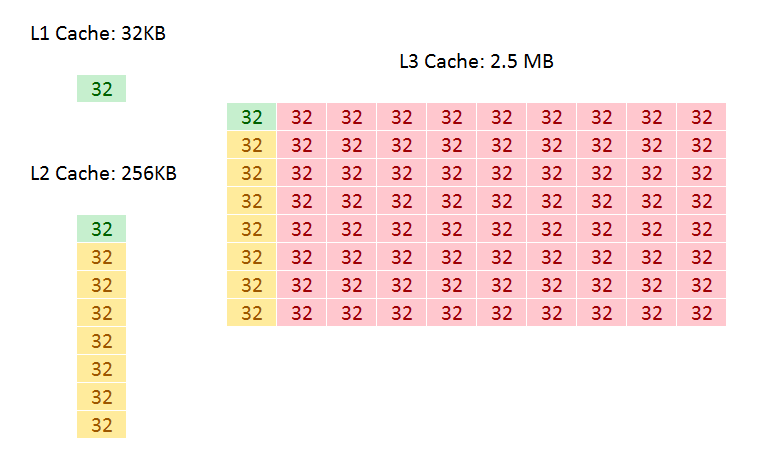
| 256 KB 4-way 11-cycle 4KB 1536-entry 12-way TLB Inclusive |
L2 | 1 MB 16-way 11-13 cycle 4KB 1536-entry 12-way TLB Inclusive |
| < 2 MB/core Up to 16-way 44-cycle Inclusive |
L3 | 1.375 MB/core 11-way 77-cycle Non-inclusive |
The new core keeps the same L1D and L1I cache structures, both implementing writeback 32KB 8-way caches for each. These caches have a 4-cycle access latency, but differ in their access support: Skylake-S does 2x32-byte loads and 1x32-byte store per cycle, whereas Skylake-SP offers double on both.
The big changes are with the L2 and the L3. Skylake-SP has a 1MB private L2 cache with 16-way associativity, compared to the 256KB private L2 cache with 4-way associativity in Skylake-S. The L3 changes to an 11-way non-inclusive 1.375MB/core, from a 20-way fully-inclusive 2.5MB/core arrangement.
That’s a lot to unpack, so let’s start with inclusivity:
Inclusive Caching
An inclusive cache contains everything in the cache underneath it and has to be at least the same size as the cache underneath (and usually a lot bigger), compared to an exclusive cache which has none of the data in the cache underneath it. The benefit of an inclusive cache means that if a line in the lower cache is removed due it being old for other data, there should still be a copy in the cache above it which can be called upon. The downside is that the cache above it has to be huge – with Skylake-S we have a 256KB L2 and a 2.5MB/core L3, meaning that the L2 data could be replaced 10 times before a line is evicted from the L3.
A non-inclusive cache is somewhat between the two, and is different to an exclusive cache: in this context, when a data line is present in the L2, it does not immediately go into L3. If the value in L2 is modified or evicted, the data then moves into L3, storing an older copy. (The reason it is not called an exclusive cache is because the data can be re-read from L3 to L2 and still remain in the L3). This is what we usually call a victim cache, depending on if the core can prefetch data into L2 only or L2 and L3 as required. In this case, we believe the SKL-SP core cannot prefetch into L3, making the L3 a victim cache similar to what we see on Zen, or Intel’s first eDRAM parts on Broadwell. Victim caches usually have limited roles, especially when they are similar in size to the cache below it (if a line is evicted from a large L2, what are the chances you’ll need it again so soon), but some workloads that require a large reuse of recent data that spills out of L2 will see some benefit.
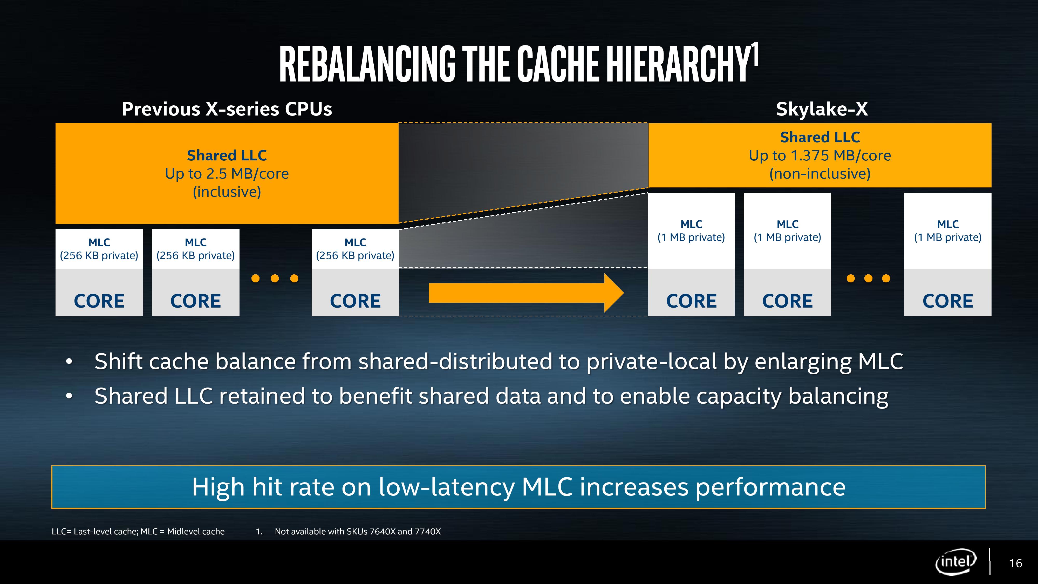
So why move to a victim cache on the L3? Intel’s goal here was the larger private L2. By moving from 256KB to 1MB, that’s a double double increase. A general rule of thumb is that a doubling of the cache increases the hit rate by 41% (square root of 2), which can be the equivalent to a 3-5% IPC uplift. By doing a double double (as well as doing the double double on the associativity), Intel is effectively halving the L2 miss rate with the same prefetch rules. Normally this benefits any L2 size sensitive workloads, which some enterprise environments such as databases can be L2 size sensitive (and we fully suspect that a larger L2 came at the request of the cloud providers).
Moving to a larger cache typically increases latency. Intel is stating that the L2 latency has increased, from 11 cycles to ~13, depending on the type of access – the fastest load-to-use is expected to be 13 cycles. Adjusting the latency of the L2 cache is going to have a knock-on effect given that codes that are not L2 size sensitive might still be affected.
So if the L2 is larger and has a higher latency, does that mean the smaller L3 is lower latency? Unfortunately not, given the size of the L2 and a number of other factors – with the L3 being a victim cache, it is typically used less frequency so Intel can give the L3 less stringent requirements to remain stable. In this case the latency has increased from 44 in SKL-X to 77 in SKL-SP. That’s a sizeable difference, but again, given the utility of the victim cache it might make little difference to most software.
Moving the L3 to a non-inclusive cache will also have repercussions for some of Intel’s enterprise features. Back at the Broadwell-EP Xeon launch, one of the features provided was L3 cache partitioning, allowing limited size virtual machines to hog most of the L3 cache if it was running a mission-critical workflow. Because the L3 cache was more important, this was a good feature to add. Intel won’t say how this feature has evolved with the Skylake-SP core at this time, as we will probably have to wait until that launch to find out.
As a side note, it is worth noting here that Broadwell-E was a 256KB private L2 but 8-way, compared to Skylake-S which was a 256KB private L2 but 4-way. Intel stated that the Skylake-S base core went down in associativity for several reasons, but the main one was to make the design more modular. In this case it means the L2 in both size and associativity are 4x from Skylake-S by design, and shows that there may be 512KB 8-way variants in the future.


264 Comments
View All Comments
rascalion - Monday, June 19, 2017 - link
Are the Ryzen numbers in the charts retests using the last round of bios and software updates?Ian Cutress - Monday, June 19, 2017 - link
As much as possible, the latest BIOSes are used.Our CPU testing suite is locked in for software versions as of March 2017. This is because testing 30/50/100+ CPUs can't be done overnight, we have to have rigid points where versions are locked in. My cycle is usually 12-18 months. (Note I'm only one person doing all this data.)
FreckledTrout - Monday, June 19, 2017 - link
Ian any chance once there are a few BIOS tweaks you could say do a mini updated review on the 7820x vs Ryzen 1800x. With Ryzen having latest BIOS as well plus 3200Mhz memory. I'm just curious really how the 8-core guys line up when some of the dust settles and I think a lot of people will be.Ian Cutress - Monday, June 19, 2017 - link
Any reason why 3200? I'll have Intel people saying it is pushing the Ryzen out of specjjj - Monday, June 19, 2017 - link
You could do a memory subsystem scaling review for all platforms, Skylake X, Threadripper, Ryzen (Summit Ridge) and Coffee Lake. Cache, interconnect, DRAM. See where they are, how they scale, where the bottlenecks are, single rank vs dual rank modules and perf impact in practice.Why not even impact on power and efficiency.In any case, you'll need to update Ryzen 5 and 7 results when Ryzen 3 arrives , isn't it?
For DRAM at 3200 it might be out of spec - overclocking the core is out of spec too but that has never stopped anyone from overclocking the memory. Right now 3200 is what a lot of folks buy , at least for higher end mainstream Ofc some will argue that Ryzen scales better with memory and that's why it is unfair but it's a hell of a lot more reasonable than testing 1080p gaming with a 1080 TI since it's a popular real world scenario.
At the end of the day the goal should be to inform, not to watch out for Intel's or AMD''s feelings.
vanilla_gorilla - Monday, June 19, 2017 - link
>For DRAM at 3200 it might be out of spec - overclocking the core is out of spec too but that has never stopped anyone from overclocking the memory.This. Exactly. We're enthusiasts and we always push the envelope. No one cares what the specs are all we care is about what these processors are capable of in the right hands.
And Ian I think you guys do an awesome job, there's no other place I look for CPU benchmarks. Keep up what you do, we all appreciate it, as well as your willingness to have a dialog with us about the process. Really cannot say how impressed I am by how open and engaged you are, it's really commendable.
Ian Cutress - Tuesday, June 20, 2017 - link
Thanks for the comments :)Though on your comments about pushing things out of spec. We have a good deal of readers who want plain stock for their businesses - AT isn't solely a consumer focused site. Otherwise I'd just jack all the CPUs and just post OC results :D Our base testing will always be at stock, and for comparison testing there has to be an element of consistency - testing an OC'ed part against a stock part in a direct A vs B comparison is only going to end up with a barrage of emails being rammed down my throat. There has to be some planning involved.
Ian Cutress - Tuesday, June 20, 2017 - link
I've been planning a memory scaling article, I just haven't had the time (this article was around 6 weeks of prep with all the events going on that I had to attend).Note we don't retest stuff every review. With our new 2017 test suite, I've been going through regression testing. Usually regression testing is done once for the full segment until the benchmarks are changed again. I'll look at my next few months (still stupidly busy) and look at the priorities here.
FreckledTrout - Monday, June 19, 2017 - link
Most people can easily buy a 3200 kit for not a lot of extra money. It doesn't take a lot tweaking(well not anymore on AGESA 1.0.0.6) or silicone lottery like an OC, just a bit more cash. From what I have seen with Ryzen it is the sweet spot on price and performance. I would assume Its likely the most chosen configuration on the R7's. To make it fair use 3200 on the 7820x as well. I only ask because Ryzen did way better than I would have thought and would like to see it with 3200Mhz memory and latest updates to see really how close Intel and AMD are on 8-core systems. Then im going to build :)tipoo - Monday, June 19, 2017 - link
Launch review! Nice work dude(s).