The Intel Skylake-X Review: Core i9 7900X, i7 7820X and i7 7800X Tested
by Ian Cutress on June 19, 2017 9:01 AM ESTDie Size Estimates and Arrangements
On the previous page, we showed pictures of ring bus and mesh arrangements. With a ring bus, ultimately the silicon layout of the cores and the interconnects can be regular but are not that stringent. Put the cores in a circle (or overlapping circles) and away you go. With a mesh, things get a little more rigid.
The mesh diagrams on the previous page are all presented as rectangles in x*y arrangements. You either have to add a full row or a full column to increase the die count, whereas in a ring it could be straight forward just to add another pair of cores into the ring (which is what happened over the last few generations). Adding a pair of cores in a mesh means that you end up with more corners and more edges – not all cores end up ‘equal’ and there can be performance penalties therein. Ideally, an arrangement where x = y is usually the best bet. This lets us make some predictions about how Intel’s silicon is lining up.
A side-note for discussion. If we had a 100x100 core arrangement, the cores in the middle would have big latency to get anywhere near external memory. Also, a 2D mesh could become a 3D mesh.
Three things come to our aid in discussing the LCC and HCC silicon. First was the original Skylake-X announcement back at Computex: one of Intel’s slides had an image of the basic floorplan of the HCC silicon to be used for the high core-count Skylake-X processors:
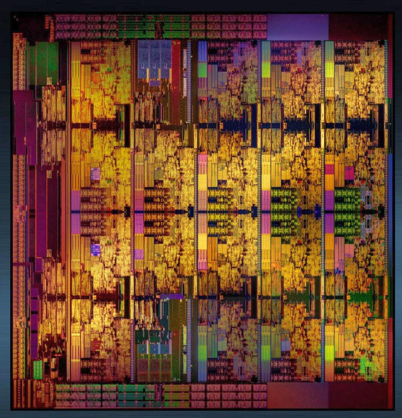
At the time, we were a bit stumped by this image. By counting the regular structures, we can see 4x5 arrangement, or rather a 20-core chip. On closer inspection two of the cores were different: on the second column, the top and bottom ‘cores’ did not look like cores. At the time we postulated that given the size of AVX512, this might be where they were. But the second piece of information was given through Intel’s mesh announcement.
Here’s the diagram:

This is meant to be a pseudo mockup of a theoretical core of n processors using the mesh topology. At the top are the socket links, along with the PCIe root complexes. However on the left and right are the DRAM controllers, essentially taking up the same area as a core but also using one of the mesh networking links.
So scoot back to that HCC die image, and zoom in on one of those odd looking ‘cores’:
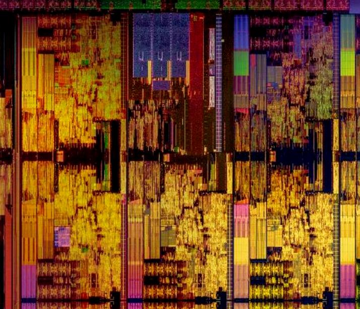
What we can see is three regular blue/green vertical areas, which means three on each side, for a total of six. Skylake-X only has four memory channels, but leaks have shown that the new Skylake-SP processors have six memory channels by design, so here they are. In the 4x5 grid, we have 18 cores and two sets of memory channels.
Back when Skylake-X was announced at Computex, I wrote that we were expecting the LCC silicon to be a 12-core design. At this time, we were still expecting Intel to use a ring-bus topology, and I mentioned before, adding two cores to a ring bus is fairly easy at the expense of peak latency between cores. Now that we know that Intel is using a mesh, it is quite different.
12 cores could quite easily fit into LCC silicon in a 3x4 arrangement, but that does not leave any room for the six memory controllers that the enterprise Xeons are all meant to have. If we added two ‘extra’ core sized areas for the 12-core design, we need a total of 14 segments. Using the x*y arrangement as required above, the only way 14 cores works is using a 7*2 arrangement. If this was the case, the DRAM controllers would essentially fill a whole row, or be at opposite ends of the column. If one of the x*y numbers is the number two, it makes more sense to use a ring bus any day of the week for power, die area and simplicity.
So that means that the 12-core SKU, the Core i9-7920X, is likely derived from the HCC 18-core silicon. Which also explains why that CPU has been delayed until August.
Die Sizes
At this point in time, the Skylake-X processors based on the LCC silicon have been in the hands of a few people. At Computex there were several extreme overclocking (using sub-zero coolants) events dedicated to the new processors. One element of recent extreme overclocking is delidding the processor and removing the integrated heat spreader to replace the thermal interface material underneath.
In general removing the IHS is not recommended without practice and experience, but for some processors in the past we have seen sizeable temperature benefits by replacing the standard thermal interface material (TIM) that Intel uses. The discussion on whether Intel should be offering a standard goopy TIM or the indium-tin solder that they used to (and AMD uses) is one I’ve run on AnandTech before, but there’s a really good guide from Roman Hartung, who overclocks by the name der8auer. I’m trying to get him to agree to post it on AnandTech with SKL-X updates so we can discuss it here, but it really is some nice research. You can find the guide over at http://overclocking.guide.
However removing the IHS means we can measure the silicon die.
The 10-core LCC die, which is a 3x4 design, measures in at 14.3 x 22.4, or 322mm2.
Using this, working from Intel’s 4x5 HCC diagram (and assuming it hasn’t been stretched), we can get 21.6 x 22.4 = 484mm2 for the high-core count design.
That leaves the Extreme core count option. Using the x*y strategy again, Intel could either run a 5x5 design, which gives 25 areas and 23 cores – which is unlikely. Next up is a 5x6 design, which gives 30 areas and 28 cores. It’s no secret that many leaks are pointing to a 28-core XCC processor at this point.
There’s also the fact that Intel provided this die shot at the Intel Manufacturing Day a few weeks ago, clearly showing the 5x6 arrangement:
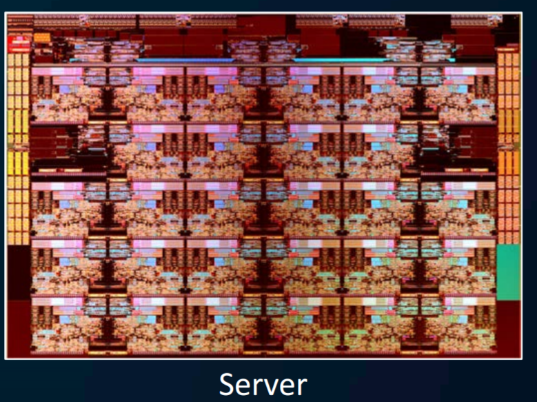
Doing the basic math on a 5x6 design gives us a 21.6 x 32.3 = 698mm2 die size for XCC.
| Skylake-SP Die Sizes | |||
| Arrangement | Dimensions (mm) |
Die Area (mm2) |
|
| LCC | 3x4 (10-core) | 14.3 x 22.4 | 322 mm2 |
| HCC | 4x5 (18-core) | 21.6 x 22.4 | 484 mm2 |
| XCC | 5x6 (28-core) | 21.6 x 32.3 | 698 mm2 |
Compared to other chips with Intel’s mesh architecture, Knights Landing comes in at 646mm2 (minus MCDRAM), and sources put Knights Corner at 720mm2.


264 Comments
View All Comments
rascalion - Monday, June 19, 2017 - link
Are the Ryzen numbers in the charts retests using the last round of bios and software updates?Ian Cutress - Monday, June 19, 2017 - link
As much as possible, the latest BIOSes are used.Our CPU testing suite is locked in for software versions as of March 2017. This is because testing 30/50/100+ CPUs can't be done overnight, we have to have rigid points where versions are locked in. My cycle is usually 12-18 months. (Note I'm only one person doing all this data.)
FreckledTrout - Monday, June 19, 2017 - link
Ian any chance once there are a few BIOS tweaks you could say do a mini updated review on the 7820x vs Ryzen 1800x. With Ryzen having latest BIOS as well plus 3200Mhz memory. I'm just curious really how the 8-core guys line up when some of the dust settles and I think a lot of people will be.Ian Cutress - Monday, June 19, 2017 - link
Any reason why 3200? I'll have Intel people saying it is pushing the Ryzen out of specjjj - Monday, June 19, 2017 - link
You could do a memory subsystem scaling review for all platforms, Skylake X, Threadripper, Ryzen (Summit Ridge) and Coffee Lake. Cache, interconnect, DRAM. See where they are, how they scale, where the bottlenecks are, single rank vs dual rank modules and perf impact in practice.Why not even impact on power and efficiency.In any case, you'll need to update Ryzen 5 and 7 results when Ryzen 3 arrives , isn't it?
For DRAM at 3200 it might be out of spec - overclocking the core is out of spec too but that has never stopped anyone from overclocking the memory. Right now 3200 is what a lot of folks buy , at least for higher end mainstream Ofc some will argue that Ryzen scales better with memory and that's why it is unfair but it's a hell of a lot more reasonable than testing 1080p gaming with a 1080 TI since it's a popular real world scenario.
At the end of the day the goal should be to inform, not to watch out for Intel's or AMD''s feelings.
vanilla_gorilla - Monday, June 19, 2017 - link
>For DRAM at 3200 it might be out of spec - overclocking the core is out of spec too but that has never stopped anyone from overclocking the memory.This. Exactly. We're enthusiasts and we always push the envelope. No one cares what the specs are all we care is about what these processors are capable of in the right hands.
And Ian I think you guys do an awesome job, there's no other place I look for CPU benchmarks. Keep up what you do, we all appreciate it, as well as your willingness to have a dialog with us about the process. Really cannot say how impressed I am by how open and engaged you are, it's really commendable.
Ian Cutress - Tuesday, June 20, 2017 - link
Thanks for the comments :)Though on your comments about pushing things out of spec. We have a good deal of readers who want plain stock for their businesses - AT isn't solely a consumer focused site. Otherwise I'd just jack all the CPUs and just post OC results :D Our base testing will always be at stock, and for comparison testing there has to be an element of consistency - testing an OC'ed part against a stock part in a direct A vs B comparison is only going to end up with a barrage of emails being rammed down my throat. There has to be some planning involved.
Ian Cutress - Tuesday, June 20, 2017 - link
I've been planning a memory scaling article, I just haven't had the time (this article was around 6 weeks of prep with all the events going on that I had to attend).Note we don't retest stuff every review. With our new 2017 test suite, I've been going through regression testing. Usually regression testing is done once for the full segment until the benchmarks are changed again. I'll look at my next few months (still stupidly busy) and look at the priorities here.
FreckledTrout - Monday, June 19, 2017 - link
Most people can easily buy a 3200 kit for not a lot of extra money. It doesn't take a lot tweaking(well not anymore on AGESA 1.0.0.6) or silicone lottery like an OC, just a bit more cash. From what I have seen with Ryzen it is the sweet spot on price and performance. I would assume Its likely the most chosen configuration on the R7's. To make it fair use 3200 on the 7820x as well. I only ask because Ryzen did way better than I would have thought and would like to see it with 3200Mhz memory and latest updates to see really how close Intel and AMD are on 8-core systems. Then im going to build :)tipoo - Monday, June 19, 2017 - link
Launch review! Nice work dude(s).