Exploring DynamIQ and ARM’s New CPUs: Cortex-A75, Cortex-A55
by Matt Humrick on May 29, 2017 12:00 AM EST- Posted in
- Smartphones
- CPUs
- Arm
- Mobile
- Cortex
- DynamIQ
- Cortex A75
- Cortex A55
Cortex-A75 Microarchitecture
The Cortex-A75 is the newest member of ARM’s Sophia family of CPUs, which also includes the A73, A17, and A12. It’s no surprise then that the A75 and A73 have much in common just like the A72 and A57 before them (both of which belong to the Austin CPU family); however, ARM’s focus has shifted from improving power efficiency and thermal headroom for A73 to improving performance and adding new features for A75. ARM addressed its performance goals through significant changes to the pipeline and support for DynamIQ, while the new features are a byproduct of moving from the ARMv8.0 architecture to ARMv8.2. For this article, I’m primarily going to focus on what’s new for A75, so I recommend reading our introduction to the A73 to get a more complete understanding of the A75 microarchitecture.
The A75 uses a relatively short 11-13+ stage (depending on instruction type) out-of-order pipeline similar to the A73. Instruction fetch is still 4 stages and the decoder is still able to decode most instructions in a single cycle, with µops destined for the NEON/FP (floating-point) pipelines requiring an additional decode stage; however, moving to 3-wide decode makes the A75 is a wider machine than A73, a big change that will be discussed in greater detail below.
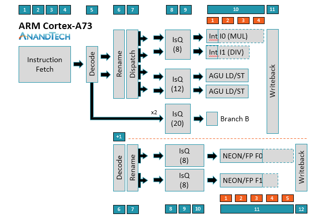
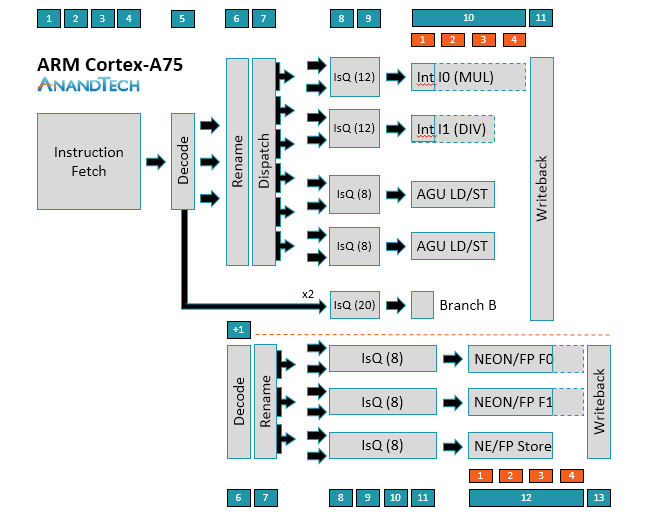
The ability to decode up to 3 instructions/cycle means A75 can now dispatch up to 6 µops/cycle instead of 4 µops/cycle for A73. On the integer side, the A75 can feed up to 2 µops into each issue queue. Instead of shared issue queues for the 2 ALUs and 2 AGUs, each pipe in A75 gets its own issue queue with more entries. This allows the A75 to be more speculative, improving its ability to execute instructions out of order and continue operation during an L1 D-cache miss that hits in L2, for example. The peak issue rate increases to 8 µops/cycle, 1 for each pipe.
As the diagrams for A73/A75 show, simple branch µops can bypass Rename and Dispatch, effectively removing 2 stages of latency; however, more complex branch instructions that require access to registers can spawn additional branch, AGU, and ALU µops that require passing through Rename/Dispatch, with some additional complexity hidden within the Rename stage.
Moving to the NEON/FP side, you’ll notice that there’s no Dispatch stage for A73/A75. Obviously, µops are still being pushed into the issue queues, and there’s still load balancing between queues, but it’s handled differently and one reason why the issue queues are 1-2 stages longer than those on the integer side.
There have been some changes to the NEON/FP side as well. The A75 can now “dispatch” up to 3 µops/cycle and sink up to 2 µops into each issue queue, which grow to 4 stages deep instead of 3 for A73. ARM looked at increasing the number of entries in the issue queues too, but it found this increased power more than performance, so it nixed the idea. Instead it added a dedicated NEON/FP store pipe with its own issue queue. The latency of a FP multiply-accumulate (MAC) has also been reduced to 5 cycles compared to 6 cycles on A73.
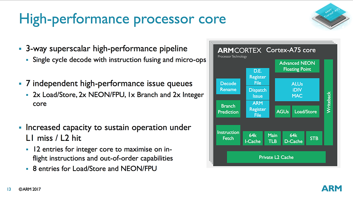
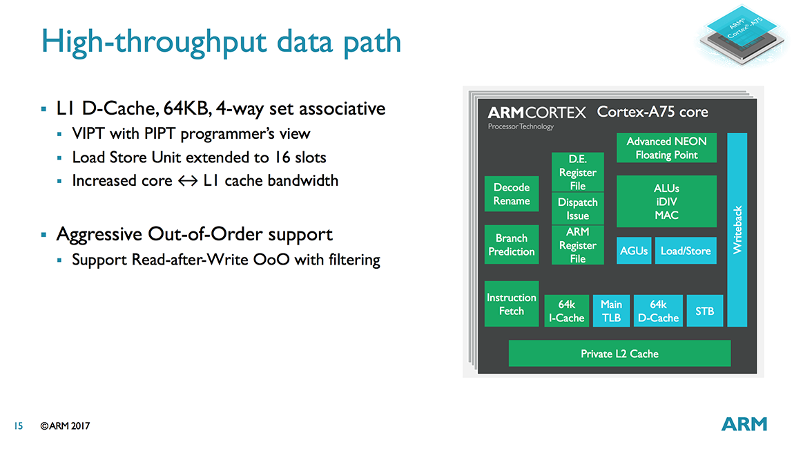
I’ll discuss the execution pipelines in greater detail as we work our way through the data path, but let’s start on the instruction side first. The A75 is still a “slot-based microarchitecture,” which was first introduced with the A73. ARM is not disclosing any additional details beyond its basic explanation from last year, namely that there are 8 “slots” that work to eliminate redundant access to resources within the instruction block, which ultimately reduces power consumption.
Both the A73 and A75 have a very simple instruction prefetcher that feeds into a fixed 64KB L1 I-cache that is 4-way set associative and uses a VIPT (Virtually Indexed, Physically Tagged) access scheme, common for L1 caches because of their sensitivity to latency.
The A73 received a completely new main branch predictor, along with a new 64-entry micro-BTAC for accelerating predictions. In addition to the main predictor, there’s also a static branch predictor, which is used as a fallback when the main predictor has insufficient history, and a return stack, which contains nested subroutine return addresses. An indirect predictor, which is only used when necessary (reducing its power penalty because indirect branches occur less frequently), uses a 2-way 256-entry BTAC (Branch Target Address Cache).
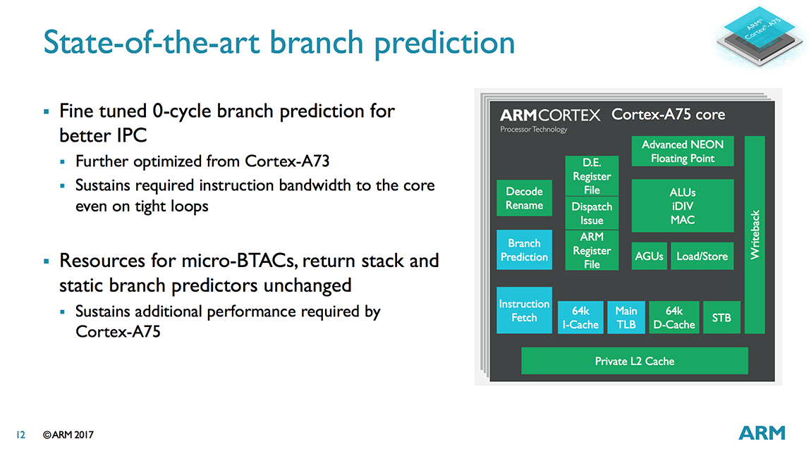
While designing the A75, ARM found that the A73’s branch predictor still performed well and that improving performance further resulted in diminishing returns, with power climbing faster than performance; therefore, the A73’s predictor was carried over to the A75. ARM did fine tune the 0-cycle micro-predictors, which sit upstream of the main predictor, improving IPC by further reducing the likelihood of pipeline bubbles in tight loops.
As I mentioned above, the A75 moves to a 3-wide instruction decode stage, up from 2-wide for the A73 and matching the 3-wide A72. ARM is always looking for ways to improve IPC (Instructions Per Cycle), and it noted that while running SPECint 2006 the A73 achieves an IPC of roughly 1.2 overall, increasing to 1.6 to 1.8 at specific sections within the test and dipping to 0.4 to 0.6 in others. Even much larger CPUs achieve an average IPC of just over 2. This does not mean you only need a 2-wide decoder, however, because there are situations that require greater throughput. For example, after a branch mispredict that requires a pipeline flush—which may occur 2-4 times for every 1000 instructions—the CPU needs to refill the issue queues as fast as possible so it can begin extracting ILP. So going wider helps throughput when you need a sudden burst of instructions. There’s a power and area penalty for going wider of course, because it causes a ripple effect through the rest of the pipeline, but it was clear to ARM that moving to 3-way superscalar was necessary to meet its IPC goals.
The A75’s Rename and Dispatch stages are similar to the A73’s. Like the A73 and other Sophia CPUs, there’s no reorder buffer or architectural register file in the A75. Instead it uses a physical register file for storing µop operands, reducing power by limiting the amount of data moving around the CPU and eliminating some instruction window bottlenecks that arise from using a reorder buffer.
The A75 does see some optimizations here, including the ability for loads to bypass writes, improving the core’s ability to execute out of order and better cope with an L2 cache miss. ARM also found that certain instructions that get cracked during the decode stage (because they need access to the register file during rename) were using too many entries in the A73’s issue queues, so the A75 now recombines these back into a single instruction after the rename stage, freeing up space in the issue queues for other µops.
Moving over to the data path, we find an improved data prefetcher. The L1 and L2 prefetchers were already overhauled for A73, but the stride prefetcher has been retuned to better handle out of order execution for A75.
The 64KB L1 D-cache carries over nearly unchanged from A73. This is VIPT like the L1 I-cache, which reduces latency by performing the cache index lookup in parallel with the TLB translation. The A73/A75 handle aliasing issues, where several virtual addresses might reference the same physical address, in hardware, making the 4-way set associative VIPT cache look like a PIPT 8-way 32kB or 16-way 64KB cache to the programmer.
The A75 gets an integrated L2 cache that operates at core speed, reducing latency by more than 50% compared to the A73 that shares an L2 cache with the other CPUs in the same cluster. For instruction fetch, latency drops from 20-25 cycles to 11 cycles (10 cycle for a L1 miss, L2 hit), and for the lowest latency scenario (a load that forwards to the AGU because of a dependent load address) latency drops from 19 cycles to 8 cycles.
The optional L2 cache can be either 256KB or 512KB. Choosing the 512KB option only improves performance by about 2% compared to 256KB for a single core, but provides a better 4-5% uplift when using 4 A75 cores with DynamIQ. The L1 D-cache and L2 are now fully-exclusive instead of pseudo-exclusive like A73, which saves area because data is not duplicated in the L2 cache. The L1 I-cache is pseudo-inclusive.
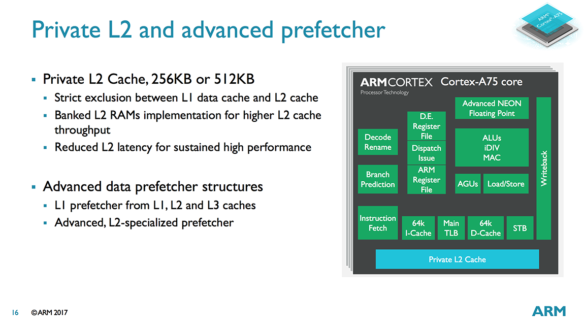
ARM improved the overall L2 hit rate by biasing the L2 cache replacement policy to have a higher affinity for instructions. The L2’s higher hit rate and lower latency improves performance but also saves power and area by allowing the A75 to continue using a very simple instruction prefetcher.
The A75’s main TLB is now non-blocking with a two outstanding fetch capability including hit under miss (the A73 main TLB is a blocking design). This change improves performance when there’s a TLB miss requiring a page table walk in main system memory. With a non-blocking TLB, it can continue to process translation requests while waiting for the page table walk to complete, which takes a comparatively long time because it requires multiple memory accesses.
Our trip through the data side of the A75’s memory system ends with the AGUs (Address Generation Units). Another carry over from the A73, the two AGUs are capable of performing both loads and stores, offering greater flexibility and a higher issue rate into the memory system. The size of the store buffer (STB), where all stores are pushed once they’ve been committed and are no longer speculative, increases to 7 128-bit slots.
Now it’s time to shift our focus to the execution pipelines. The A75’s ALU/INT pipes are the same as A73. Both ALUs can perform basic operations such as additions and shifts, but only one ALU handles integer multiplication and multiply-accumulate operations, while the other focuses on integer division with a Radix-16 divider. This means the A73/A75 cannot perform two integer multiplies or divides in parallel, but it can dual issue a MUL/MAC alongside a divide/add/shift. While nearly all instructions complete in 1 or 2 cycles, more complex integer multiplication and division operations require additional cycles. It’s interesting that after making the move to 3-wide decode, ARM considered adding a third ALU/INT pipe; however, the performance increase was not enough to justify the increase in power.
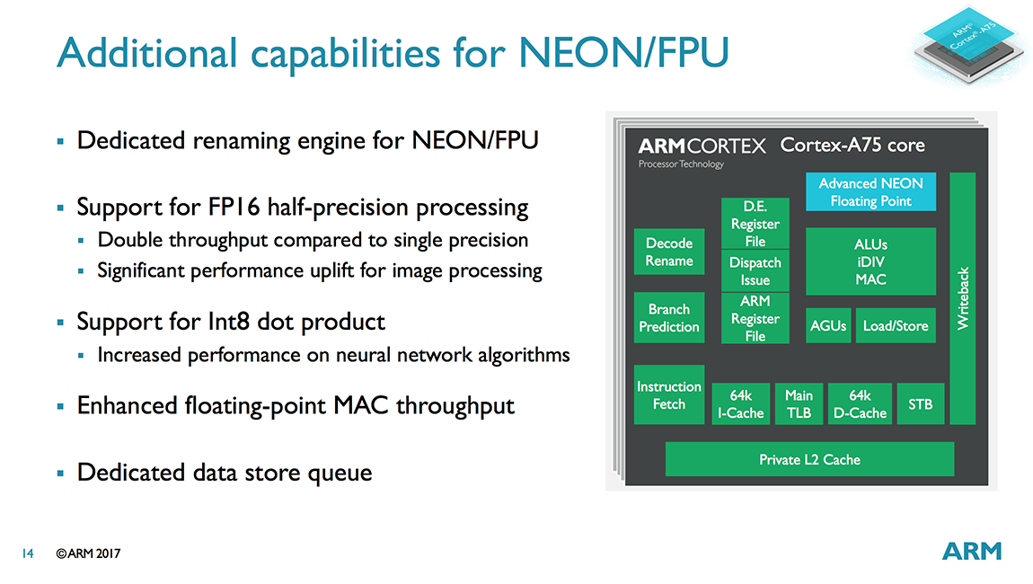
The 2 64-bit NEON/Floating Point pipes have their own dedicated Rename stage and 128-bit register file, with each SIMD NEON pipe in the A73/A75 capable of performing 8 8-bit integer, 4 16-bit integer, 2 32-bit integer or single-precision floating-point (FP), or 1 64-bit integer or double-precision FP operations per cycle, giving programmers the flexibility to choose the right balance between precision and performance.
The A75 also gains native support for half-precision FP16 operations by updating to the ARMv8.2 architecture. Using less precise data types (16-bits for FP16 versus 32- or 64-bits) reduces the amount of memory/cache required to store data and improves memory bandwidth, which can be a desirable trade-off for certain applications like machine learning and image processing. The A73 and earlier big cores could fetch FP16 values, but they need to be converted to FP32 before execution, resulting in some additional overhead.
Looking to improve performance, many neural-network algorithms are dropping down to 8-bit precision, especially after training is complete. To speed up these algorithms, the A75 (courtesy of the ARMv8.2 architecture) includes a new INT8 dot product instruction, which combines multiple instructions that required being executed back to back to back into a single instruction, significantly improving latency.
Starting with the A73 microarchitecture, ARM worked to improve IPC by moving to 3-wide decode and improving the core’s out-of-order capability, while DynamIQ support means a higher performing integrated L2 cache backed by a new L3 cache. The ARMv8.2 architecture also provides new features and new NEON instructions for accelerating neural networks and image processing.


104 Comments
View All Comments
Samus - Monday, May 29, 2017 - link
Ok, point taken, 4 year gap. Even more unacceptable. But you continue to imply the architecture hitting a wall because of the inherently in order nature of RISC so I ask you, why have Samsung and Apple continued to have great success deviating from ARM's reference designs, while Qualcomm has been married to them and paying the performance price (specifically looking at you, 808)Death666Angel - Monday, May 29, 2017 - link
"die-constrained design" He gave the answer right there, at least as far as Apple is concerned. ARM is imposing a certain, small, die size for the A53/55 cores, that limits their potential performance a lot. Apple doesn't care about die size since their margins are high enough. The Apple A5X was as large as the Intel Ivy Bridge 4C die. Both were around in 2012, though Intel had the process node advantage. Still insane numbers. And Samsung is also very vertically integrated, they don't have to worry as much about die size as Qualcomm since they own the manufacturing as well. And QC doesn't have to play the performance game, since their choke hold on the modem technology allows them to still have plenty of design wins for the moment.Wilco1 - Monday, May 29, 2017 - link
It's a 3 year gap. And Samsung still uses Cortex-A53 alongside Mongoose.tipoo - Monday, May 29, 2017 - link
Not RISC constrained to in-order, nothing to do with RISC, rather that in-order is a design choice for this particular model for power and die size.A75, Hurricane, etc are of course massively out of order ARM/RISC designs.
name99 - Wednesday, May 31, 2017 - link
Zephyr is NOT a massive OoO design. Probably 2-wide in order. We don't know its performance, but it certainly saves power (compared toA9) while not seeming to slow down the phone.ARM seems to hurt itself by an insistence on these TINY designs. (Just like Intel on the other side hurts itself by an insistence on designs that are first server targeted). Apple wins partially by not trying to be everything to everyone...
helvete - Wednesday, August 30, 2017 - link
Ending up being nothing for nobody? /saryonoco - Monday, May 29, 2017 - link
There is nothing inherently in-order about RISC. Various ARM designs such as Cortex A57, A72, A73 and A75 are out of order.Samsung has not really deviated from ARM's reference design by much, they still use the Cortex A53 in various SoCs including their latest and greatest Exynos 8895. And that 8895 is also falling behind Snapdragon 835, which is a standard A73 implementation for all intents and purposes (Qualcomm's marketing notwithstanding).
Apple, well, they can afford to dedicate the die area to a big core. No one else can.
ZeDestructor - Tuesday, May 30, 2017 - link
Everyone can go for the giant-die approach, but thanks to how marketing works, people will buy 8 A53s well before they even consider 4 A53 + 1 Cyclone-sized core.name99 - Wednesday, May 31, 2017 - link
Ding ding ding. We have a winnerWilco1 - Monday, May 29, 2017 - link
It was late 2014, and the first designs should appear late this year (just like Cortex-A73 was announced last year and appeared the same year). That is a 3 year gap, not 4 years.Note Cortex-A53 scaled quite well, from 1.3GHz in Exynos 5433 to 1.8GHz in Kirin (and goes up to 2.5GHz in Helio P25). The big cores scaled via yearly new micro-architectures, so the big/little performance ratio has remained similar.
> Fact is, there is only so much you can do with an in-order die-constrained design.
And more importantly not only keeping but actually improving power efficiency. It could go much faster if it were allowed a similar power budget as the big cores.