The AMD Ryzen 5 1600X vs Core i5 Review: Twelve Threads vs Four at $250
by Ian Cutress on April 11, 2017 9:00 AM ESTRyzen 5, Core Allocation, and Power
In our original review of Ryzen 7, we showed that the underlying silicon design of the Ryzen package consists of a single eight-core Zeppelin die with Zen microarchitecture cores.
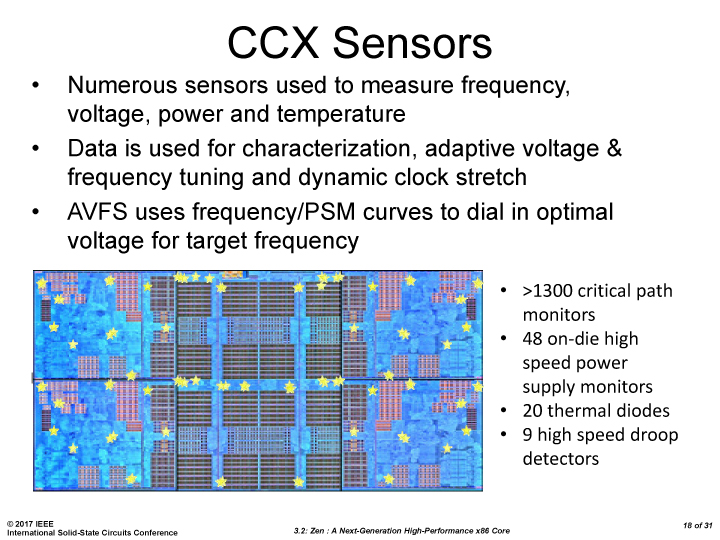
The silicon design consists of two core complexes (CCX) of four cores apiece. Each CCX comes with 512 KB of L2 cache per core, which is disabled when a core is disabled, and each CCX has 8MB of L3 cache which can remain enabled even when cores are disabled. This L3 cache is an exclusive victim cache, meaning that it only accepts evicted L2 cache entries, rather than loading data straight into it (which is how Intel builds their current L3 cache designs).
One of the suggestions regarding Ryzen 7’s performance was about thread migration and scheduling on the core design, especially as core-to-core latency varies depending on where the cores are located (and there’s a jump between CCXes). Despite the use of AMD’s new Infinity Fabric, which is ultimately a superset of HyperTransport, there is still a slightly longer delay jumping over that CCX boundary, although the default Windows scheduler knows how to manage that boundary as demonstrated by Allyn at PCPerspective.
So when dealing with a four-core or six-core CPU, and the base core design has eight-cores, how does AMD cut them up? It is possible for AMD to offer a 4+0, 3+1 or 2+2 design for its quad-core parts, or 4+2 and 3+3 variants for its hexacore parts, similar to the way that Intel cuts up its integrated graphics for GT1 variants.
There are some positives and negatives to each configuration, some of which we have managed to view through this review. The main downside from high level to a configuration split across CCXes, such as a 2+2 or 3+3, is that CCX boundary. Given that the Windows scheduler knows how to deal with this means this is less of an issue, but it is still present.
There are a couple of upsides. Firstly is related to binning – if the 2+2 chips didn’t exist, and AMD only supported 4+0 configurations, then if the binning of such processors was down to silicon defects, fewer silicon dies would be able to be used, as one CCX would have to be perfect. Depending on yield this may or may not be an issue to begin with, but having a 2+2 (and AMD states that all 2+2 configs will be performance equivalent) means more silicon available, driving down cost by having more viable CPUs per wafer out of the fabs.
Secondly, there’s the power argument. Logic inside a processor expends energy, and more energy when using a higher voltage/frequency. When placing lots of high-energy logic next to each other, the behavior becomes erratic and the logic has to reduce in voltage/frequency to remain stable. This is why AVX/AVX2 from Intel causes those cores to run at a lower frequency compared to the rest of the core. A similar thing can occur within a CCX: if all four cores of a CCX are loaded (and going by Windows Scheduler that is what happens in order), then the power available to each core has to be reduced to remain stable. Ideally, if there’s no cross communication between threads, you want the computation to be in opposite cores as threads increase. This is not a new concept – some core designs intentionally put in ‘dark silicon’ - silicon of no use apart from providing extra space/area between high power consuming logic. By placing the cores in a 2+2 and 3+3 design for Ryzen 5, this allows the cores to run at a higher power than if they were in 4+0 and 4+2 configurations.
Here’s some power numbers to show this. First, let’s start with a core diagram.
Where exactly the 0/1/2/3 cores are labelled is not really important, except 0-3 are in one CCX and 4-7 are in another CCX. As we load up the cores with two threads each, we can see the power allocation change between them. It is worth noting that the Ryzen cores have a realistic voltage/frequency limit near 4.0-4.1 GHz due to the manufacturing process – getting near or above this frequency requires a lot of voltage, which translates into power.
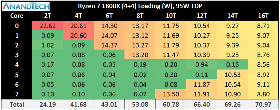
First up is the 1800X, which is a 4+4 configuration with a maximum TDP of 95W. One fully loaded core gets 22.6W, and represents the core at its maximum frequency with XFR also enabled. The same thing happens with two cores fully loaded, but at 20.6 W apiece. Moving onto three cores loaded is where XFR is disabled, and we see the drop to 3.7 GHz is saving power, as we only consume +1.33W compared to the two cores loaded situation. Three to four cores, still all on the same CCX, shows a decrease in power per core.
As we load up the first core of the second CCX, we see an interesting change. The core on CCX-2 has a bigger power allocation than any core in CCX-1. This can be interpreted in two ways: there is more dark silicon around, leading to a higher potential for this core on CCX-2, or that more power is required given the core is on its own. Technically it is still running at the same frequency as the cores on CCX1. Now as we populate the cores on CCX-2, they still consume more power per core until we hit the situation where all cores are loaded and the system is more or less equal.
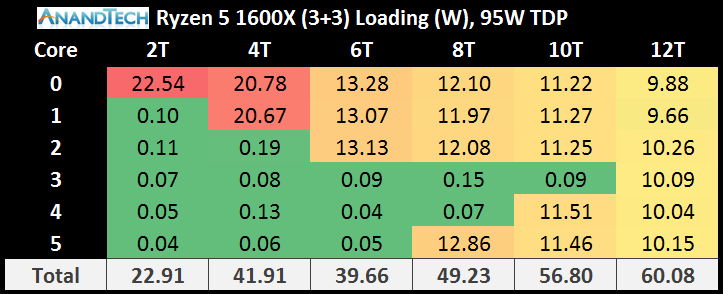
Moving to the Ryzen 5 1600X, which is a 3+3 configuration, nets more of the same. During XFR with one or two cores loaded, the power consumption is high. As we move onto the second CCX, the cores on CCX-2 consumer more power per core than those already loaded on CCX-1.
It is worth noting here that the jump from two cores loaded to three cores loaded on the 3+3 gives a drop in the total power consumption of the cores. Checking my raw data numbers, and this also translates to a total package power drop as well, showing how much extra effort it is to run these cores near 4.0 GHz with XFR enabled.
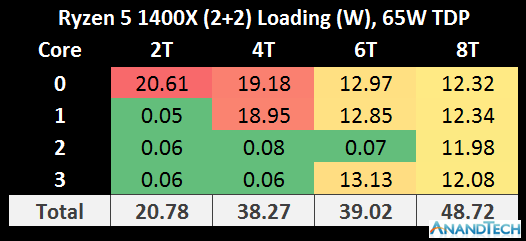
On the Ryzen 5 1500X, using a 2+2 configuration, the situation is again duplicated. The hard comparison here is the 2+2 of the 1500X to the 4+0 on the 1800X, because the TDP of each of the processors is different.
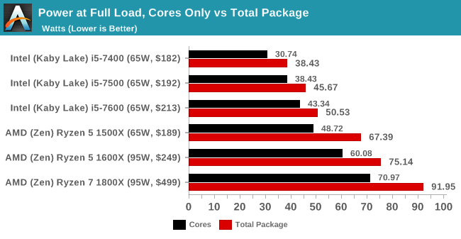
It should be noted however the total package power consumption (cores plus IO plus memory controller and so on) is actually another 10W or so above these numbers per chip.
The cache configurations play an important role in the power consumption numbers as well. In a 3+3 or a 2+2 configuration, despite one or two cores per CCX being disabled, the L3 cache is still fully enabled in these processors. As a result, cutting 25% of the cores doesn’t cut 25% of the total core power, depending on how the L3 cache is being used.
Nonetheless, the Ryzen 5 1600X, despite being at the same rated TDP as the Ryzen 7 1800X, does not get close to matching the power consumption. This ropes back into the point at the top of the page – usually we see fewer cores giving a higher frequency to match the power consumption with parts that have more cores. Because the silicon design has such a high barrier to get over 4.0 GHz with voltage and power, AMD has decided that it is too big a jump to remain stable, but still given the 1600X the higher TDP rating anyway. This may be a nod to the fact that it will cause users to go out and buy bigger cooling solutions, providing sufficient headroom for Turbo modes and XFR, giving better performance.
Despite this, we see the 1800X and 1500X each tear their TDP rating for power consumption (92W vs 95W and 67W vs 65W respectively).
However, enough talking about the power consumption. Time for benchmarks!


254 Comments
View All Comments
SkipPerk - Wednesday, May 3, 2017 - link
These are low-end CPU's. People use those for gaming and web-surfing. I have a proper Xeon machine at work like a normal person. Not to mention, you reference video software. What tiny percentage of computer users ever own or use video software? That is a tiny industry. It reminds me of the silly youtube reviews where the reviewer assumes everyone is editing videos, when less than one percent of us will ever do so.Most people buying non-Xeon CPU's really will be using basic software (MS Office, WinZip,...) or games. The only time I have used non-Xeon CPU's for work was when I had software that loved clock speed. Then I got a bunch of 6-core's and overclocked them (it was funny to watch the guys at Microcenter as I bought ten $1k CPUs and cheesy AIO water coolers). Otherwise one uses the right tool for the job.
AndrewJacksonZA - Tuesday, April 11, 2017 - link
On the last page, "On The Benchmark Results""Looking at the results, it’s hard to notice the effect that 12 threads has on multithreaded CPU tests."
Don't you mean that it's NOT hard to notice?
Drumsticks - Tuesday, April 11, 2017 - link
I didn't see the 7600k in gaming benchmarks, was that a mistake/not ready, or is it on purpose?Thanks for the review guys! This new benchmark suite looks phenomenal!
mmegibb - Tuesday, April 11, 2017 - link
I was disappointed not to see the i5-7600k in the gaming benchmarks. Perhaps it wouldn't be much different than the i5-7600, but I have sometimes seen a difference. For my next build, it's looking like it's between the 1600x and the 7600k.fanofanand - Tuesday, April 11, 2017 - link
"Platform wise, the Intel side can offer more features on Z270 over AM4"Aside from Optane support, what does Z270 offer that AM4 doesn't?
MajGenRelativity - Tuesday, April 11, 2017 - link
Z270 has more PCIe lanes off the chipset for controllers and such that AM4 does notfanofanand - Tuesday, April 11, 2017 - link
I won't disagree with that, but I'm not sure a few extra pci-e lanes is considered a feature. Features are typically something like M.2 support, built-in wifi, things like that. The extra pci-e lanes allows for MORE connected devices, but is a few extra pci-e lanes really considered a feature anymore? With Optane being worthless for 99.99999% of consumers, I'm just not seeing where Z270 gives more for the extra money.JasonMZW20 - Tuesday, April 11, 2017 - link
Let's do a rundown:Ryzen + X370
20 (3.0) + 8 (2.0)
Platform usable total: 28
Core i7 + Z270
16 + 14 (all 3.0)
Platform usable total: 30
Intel's Z270 spec sheet is a little disingenuous, as yes it does have a maximum of 24 lanes, but 10 are reserved for actual features like SATA and USB 2.0/3.x. 14 can be used by a consumer, giving you a total of 2 NVMe x4 + 1 NVMe x2 leaving x4 for other things like actual PCIe slots. That 3rd NVMe slot may share PCIe lanes with a PCIe add-in slot, if configured that way.
Ryzen PCIe config (20 lanes): 1x16, 2x8 for graphics and x4 NVMe (or x2 SATA when NVMe is not used)
Core i7 config (16 lanes): 1x16, 2x8, or 1x8+2x4 for graphics
They're actually pretty comparable.
mat9v - Tuesday, April 11, 2017 - link
No, not more PCIEx lines, those from chipset are virtual, they all go to CPU through DMI bus that is equivalent to (at best) 4 lines of PCIEx 3.0. All those chips (Intel and AMD) offer 16 lines from CPU for graphic card, but Zen also offers 4 lines for NVMe. Chipsets are connected by DMI (in Intel) and 4 lines of PCIEx 3.0 (in AMD), so that is equal, now Intel from those DMI lines offer virtual 24 lines of PCIEx 3.0 (a laugh and half) while AMD quite correctly offers 8 lines of PCIEx 2.0 (equivalent to 4 lines of PCIEx 3.0).psychobriggsy - Wednesday, April 12, 2017 - link
Indeed. If a user is going to need more than that, they're more likely going to be plumping for a HEDT system anyway. AMD's solution is coming in a bit, but that should be able to ramp up the IO significantly.