The Intel Core i3-7350K (60W) Review: Almost a Core i7-2600K
by Ian Cutress on February 3, 2017 8:00 AM ESTTest Bed and Setup
As with every CPU launch, there are a number of different directions to take the review. We have dedicated articles comparing the IPC of the new Kaby Lake line of CPUs, as well as a look into overclocking performance as a whole. We have had almost every desktop-class CPU family since Sandy Bridge tested in our benchmark suite, although only the latest have been retested. Due to timing, we were able to test all three of the new Kaby Lake-K processors, and retest the several Skylake processors, however we do have some CPU data for comparison for Haswell, Ivy Bridge, and Sandy Bridge. It will interesting to see how the CPU performance out-of-the-box has adjusted over the last five generations.
As per our testing policy, we take each CPU and place it in a suitable high-end motherboard and equip the system with a suitable amount of memory running at the processor maximum supported frequency. This is also typically run at JEDEC sub-timings where possible. It is noted that some users are not keen on this policy, stating that sometimes the maximum supported frequency is quite low, or faster memory is available at a similar price, or that the JEDEC speeds can be prohibitive for performance. While these comments make sense, ultimately very few users apply memory profiles (either XMP or other) as they require interaction with the BIOS, and most users will fall back on JEDEC supported speeds - this includes home users as well as industry who might want to shave off a cent or two from the cost or stay within the margins set by the manufacturer. Where possible, we will extend out testing to include faster memory modules either at the same time as the review or a later date.
| Test Setup | |
| Processor | Intel Core i3-7350K (ES, Retail Stepping), 60W, $157 2 Cores, 4 Threads, 4.2 GHz |
| Motherboards | MSI Z270 Gaming M7 |
| Cooling | Cooler Master Nepton 140XL |
| Power Supply | OCZ 1250W Gold ZX Series Corsair AX1200i Platinum PSU |
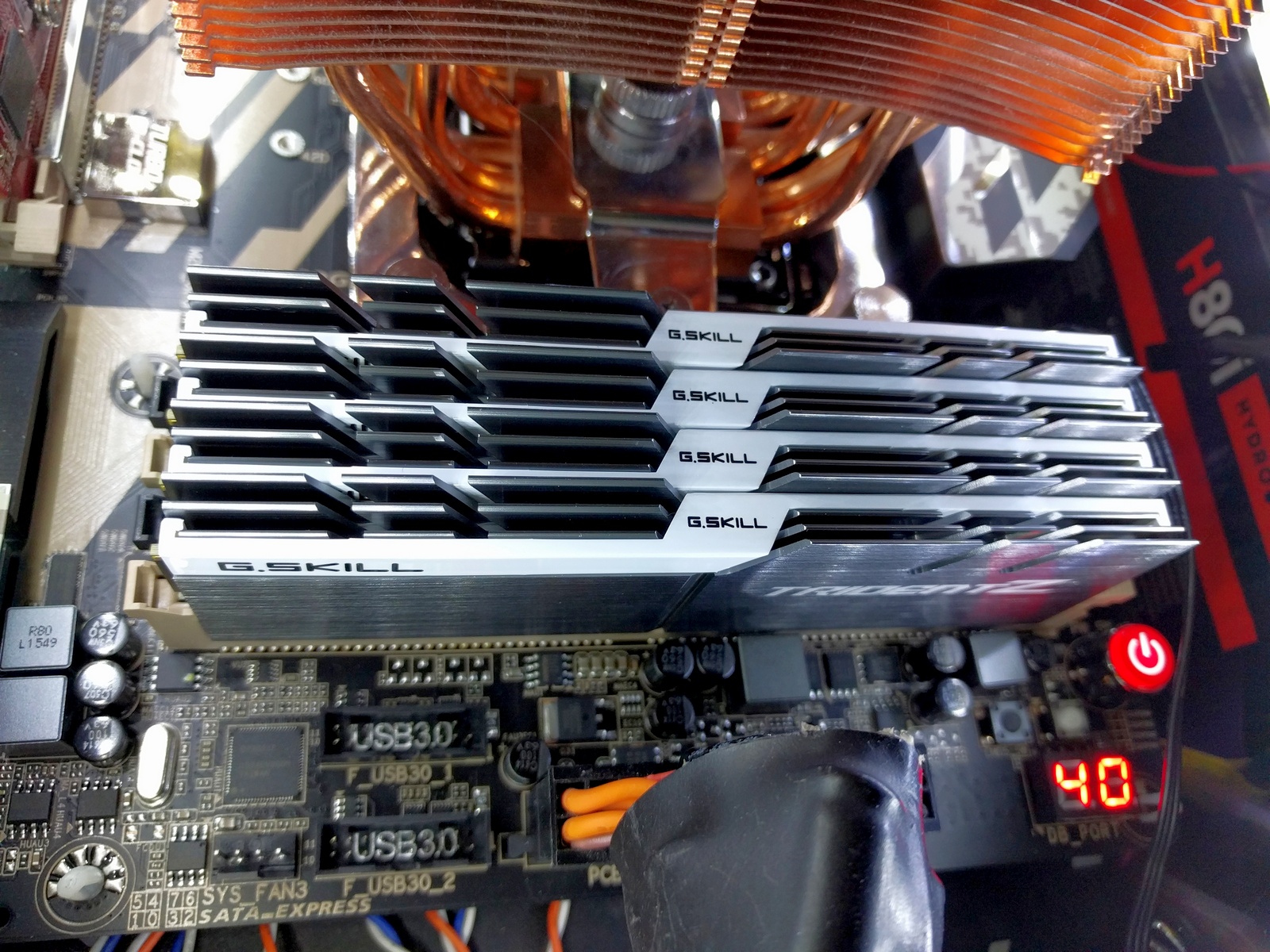
| Memory | G.Skill Ripjaws 4 DDR4-2400 C15 2x16 GB 1.2V |
| Memory Settings | DDR4-2400 C15 |
| Video Cards | ASUS GTX 980 Strix 4GB MSI R9 290X Gaming 8GB ASUS R7 240 2GB |
| Hard Drive | Crucial MX200 1TB |
| Optical Drive | LG GH22NS50 |
| Case | Open Test Bed |
| Operating System | Windows 7 64-bit SP1 |
Readers of our reviews will have noted the trend in modern motherboards to implement a form of MultiCore Enhancement / Acceleration / Turbo (read our report here) on their motherboards. This does several things, including better benchmark results at stock settings (not entirely needed if overclocking is an end-user goal) at the expense of heat and temperature. It also gives an automatic overclock which may be against what the user wants. Our testing methodology is ‘out-of-the-box’, with the latest public BIOS installed and XMP enabled, and thus subject to the whims of this feature. It is ultimately up to the motherboard manufacturer to take this risk – and manufacturers taking risks in the setup is something they do on every product (think C-state settings, USB priority, DPC Latency / monitoring priority, overriding memory sub-timings at JEDEC). Processor speed change is part of that risk, and ultimately if no overclocking is planned, some motherboards will affect how fast that shiny new processor goes and can be an important factor in the system build.
Many thanks to...
We must thank the following companies for kindly providing hardware for our multiple test beds. Some of this hardware is not in this test bed specifically, but is used in other testing.
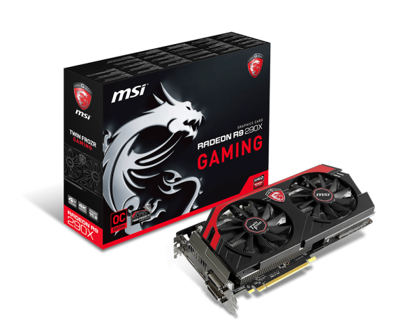
Thank you to AMD for providing us with the R9 290X 4GB GPUs. These are MSI branded 'Gaming' models, featuring MSI's Twin Frozr IV dual-fan cooler design and military class components. Bundled with the cards is MSI Afterburner for additional overclocking, as well as MSI's Gaming App for easy frequency tuning.
The R9 290X is a second generation GCN card from AMD, under the Hawaii XT codename, and uses their largest Sea Islands GPU die at 6.2 billion transistors at 438mm2 built at TSMC using a 28nm process. For the R9 290X, that means 2816 streaming processors with 64 ROPs using a 512-bit memory bus to GDDR5 (4GB in this case). The official power rating for the R9 290X is 250W.
The MSI R9 290X Gaming 4G runs the core at 1000 MHz to 1040 MHz depending on what mode it is in (Silent, Gaming or OC), and the memory at 5 GHz. Displays supported include one DisplayPort, one HDMI 1.4a, and two dual-link DVI-D connectors.
Further Reading: AnandTech's AMD R9 290X Review
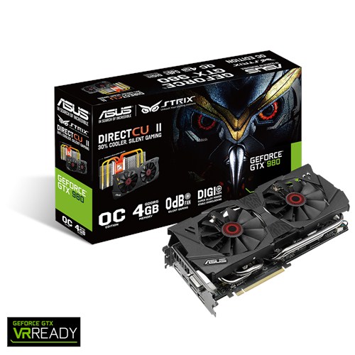
Thank you to ASUS for providing us with GTX 980 Strix GPUs. At the time of release, the STRIX brand from ASUS was aimed at silent running, or to use the marketing term: '0dB Silent Gaming'. This enables the card to disable the fans when the GPU is dealing with low loads well within temperature specifications. These cards equip the GTX 980 silicon with ASUS' Direct CU II cooler and 10-phase digital VRMs, aimed at high-efficiency conversion. Along with the card, ASUS bundles GPU Tweak software for overclocking and streaming assistance.
The GTX 980 uses NVIDIA's GM204 silicon die, built upon their Maxwell architecture. This die is 5.2 billion transistors for a die size of 298 mm2, built on TMSC's 28nm process. A GTX 980 uses the full GM204 core, with 2048 CUDA Cores and 64 ROPs with a 256-bit memory bus to GDDR5. The official power rating for the GTX 980 is 165W.
The ASUS GTX 980 Strix 4GB (or the full name of STRIX-GTX980-DC2OC-4GD5) runs a reasonable overclock over a reference GTX 980 card, with frequencies in the range of 1178-1279 MHz. The memory runs at stock, in this case 7010 MHz. Video outputs include three DisplayPort connectors, one HDMI 2.0 connector and a DVI-I.
Further Reading: AnandTech's NVIDIA GTX 980 Review
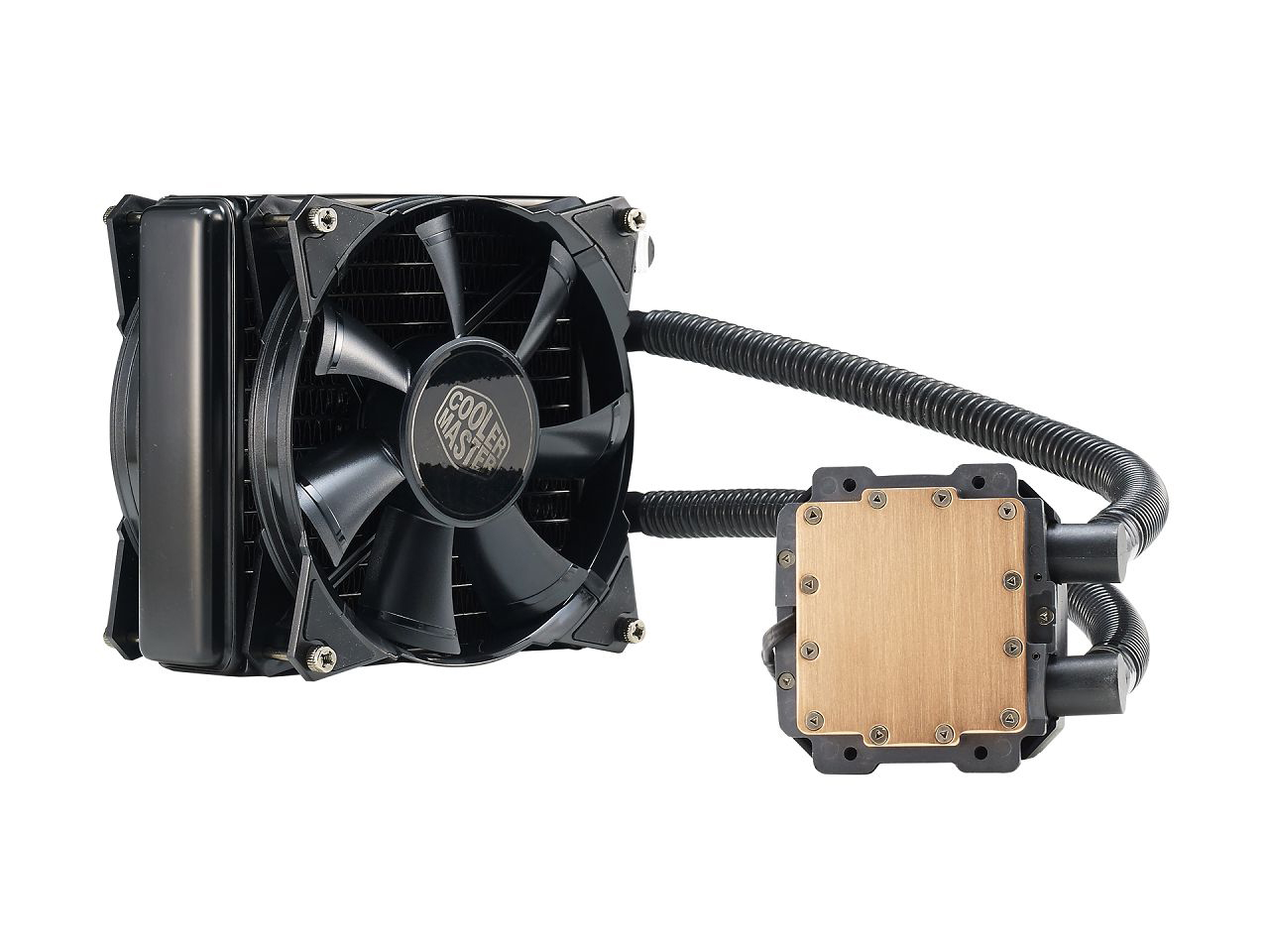
Thank you to Cooler Master for providing us with Nepton 140XL CLCs. The Nepton 140XL is Cooler Master's largest 'single' space radiator liquid cooler, and combines with dual 140mm 'JetFlo' fans designed for high performance, from 0.7-3.5mm H2O static pressure. The pump is also designed to be faster, more efficient, and uses thicker pipes to assist cooling with a rated pump noise below 25 dBA. The Nepton 140XL comes with mounting support for all major sockets, as far back as FM1, AM2 and 775.
Further Reading: AnandTech's Cooler Master Nepton 140XL Review
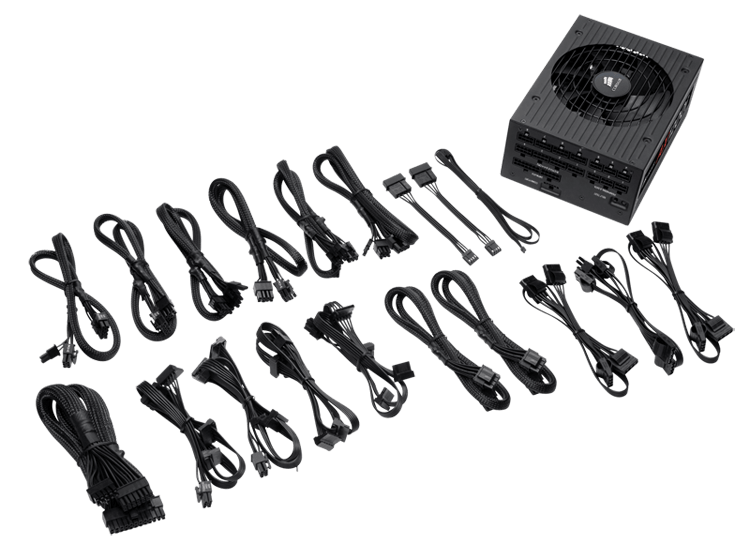
Thank you to Corsair for providing us with an AX1200i PSU. The AX1200i was the first power supply to offer digital control and management via Corsair's Link system, but under the hood it commands a 1200W rating at 50C with 80 PLUS Platinum certification. This allows for a minimum 89-92% efficiency at 115V and 90-94% at 230V. The AX1200i is completely modular, running the larger 200mm design, with a dual ball bearing 140mm fan to assist high-performance use. The AX1200i is designed to be a workhorse, with up to 8 PCIe connectors for suitable four-way GPU setups. The AX1200i also comes with a Zero RPM mode for the fan, which due to the design allows the fan to be switched off when the power supply is under 30% load.
Further Reading: AnandTech's Corsair AX1500i Power Supply Review
Thank you to Crucial for providing us with MX200 SSDs. Crucial stepped up to the plate as our benchmark list grows larger with newer benchmarks and titles, and the 1TB MX200 units are strong performers. Based on Marvell's 88SS9189 controller and using Micron's 16nm 128Gbit MLC flash, these are 7mm high, 2.5-inch drives rated for 100K random read IOPs and 555/500 MB/s sequential read and write speeds. The 1TB models we are using here support TCG Opal 2.0 and IEEE-1667 (eDrive) encryption and have a 320TB rated endurance with a three-year warranty.
Further Reading: AnandTech's Crucial MX200 (250 GB, 500 GB & 1TB) Review

Thank you to G.Skill for providing us with memory. G.Skill has been a long-time supporter of AnandTech over the years, for testing beyond our CPU and motherboard memory reviews. We've reported on their high capacity and high-frequency kits, and every year at Computex G.Skill holds a world overclocking tournament with liquid nitrogen right on the show floor. One of the most recent deliveries from G.Skill was their 4x16 GB DDR4-3200 C14 Kit, which we are planning for an upcoming review.
Further Reading: AnandTech's Memory Scaling on Haswell Review, with G.Skill DDR3-3000
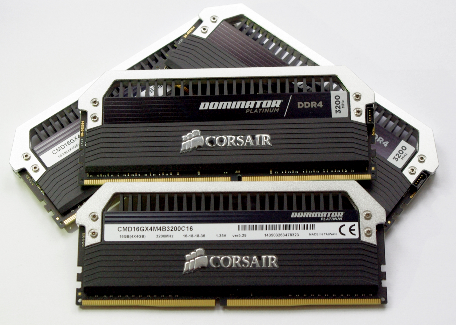
Thank you to Corsair for providing us with memory. Similarly, Corsair (along with PSUs) is also a long-time supporter of AnandTech. Being one of the first vendors with 16GB modules for DDR4 was a big deal, and now Corsair is re-implementing LEDs back on its memory after a long hiatus along with supporting specific projects such as ASUS ROG versions of the Dominator Platinum range. We're currently looking at our review pipeline to see when our next DRAM round-up will be, and Corsair is poised to participate.
Further Reading: AnandTech's Memory Scaling on Haswell-E Review


186 Comments
View All Comments
JordanV - Tuesday, February 14, 2017 - link
I think the sales argument for the big Intel chips as video encoders has been for x264 where the faster NVENC, VCE, and QuickSync technologies offer lower quality at a given bitrate for higher quality x264 settings. For most people, the hardware encoders are enough but for many others, the quality is not sufficient.The quality difference between hardware and software HEVC is smaller with higher quality software h265 encodes beating the quality of your Pascal x265 encodes but with a big performance penalty. It's not worth it for most people, but if you have limited bitrate/storage and want the best quality, it might be.
HerrKaLeun - Friday, February 3, 2017 - link
Thanks for the great review, Ian.Considering one needs an expensive Z-board to OC, for most people buying an i5 makes more sense.
I don't understand why so many people complain about Intel allegedly not making enough progress. Now you get a dual-core that comes close (or even exceeds in single threaded benches) to the former flagship quadcore. If you want to have a CPU that vastly exceeds the "old" quadcore, Intel also has newer quadcores. It is not like the i3 is the end of the lineup.... For the $317 that the 2600k used to cost you can get a KabyLake non-K i7, which sure vastly exceeds in performance (and much lower TDP). I assume someone who could afford an over $300 CPU 6 years ago can afford $300 now and upgrading to an i3 may not be what that person would do anyway. the trend goes to more cores.... most people here complain about Intel not offering mainstream hexa and octa cores... not sure why the same people allegedly are so eager to get dual-cores.
zodiacfml - Friday, February 3, 2017 - link
Dual core is too weak for me. Web browsing can use more cores.Hulk - Friday, February 3, 2017 - link
Sorry to be dense.What does 2+2, 4+2, 4+3/e mean?
babysam - Saturday, February 4, 2017 - link
The first number refers to the number of CPU cores. Te second number refers to the IGP configuration (the number of shaders, which may be a little bit different across generations, e.g. Haswell GT3 has 40 shaders, while Broadwell/Skylake GT3 have 48 shaders).The extra e means there is an extra eDRAM cache (Crystalwell) on the CPU package.
Hulk - Saturday, February 4, 2017 - link
Thanks.AndrewJacksonZA - Saturday, February 4, 2017 - link
Thank you babysam.babysam - Saturday, February 4, 2017 - link
Thank you for you article (especially when many of us are waiting on the information of new CPU of both AMD and Intel). It is always good to have something to play (overclocked) with, but this is a little bit expensive.When I read the analysis of the first page, I see the lack of information on the CPU die size and transistor count disclosed by Intel recently. Also, I feel strange that the effect of the change of the 32nm to 22nm (from Haswell to Broadwell) have such a large difference on the 2C+GT2(which Intel claims there is a 37% reduction of the die, which can be seen in the table) and the 4C+GT3(which the difference are much smaller) CPU die. I feel even stranger when I see the Skylake 4C+GT3e die is a bit smaller than the Broadwell 4c+GT3e die. So I am quite curious on the sources of the die estimate.
P.S. I found the origin of the 234mm^2 of the Skylake die size estimate.
https://techreport.com/forums/viewtopic.php?t=1177...
which based on the images of the following
http://www.anandtech.com/show/10281/intel-adds-cry...
It seems that the die described is the Skylake-H(which is a 4C+GT4e configuration). This makes the 241.5mm^2 estimate of the Broadwell 4C+GT3e a little bit unrealistic (Skylake GT4e have 72 shaders, while Broadwell GT3e have 48 only)
babysam - Saturday, February 4, 2017 - link
Just find the die size of the Broadwell-H (4C+3e) in this documenthttp://www.intel.com/content/www/us/en/embedded/pr...
According to the document, the die size of Broadwell-H (4C+GT3e) should be 13.7mmx12.3mm = 168.51mm^2
(Many thanks for the hints: https://forums.anandtech.com/threads/broadwell-cor... , which the got the answer two years ago.)
WoodyBL - Saturday, February 4, 2017 - link
Am I the only one noticing that the i5-4690 was beating the i5-7600k in a lot of benchmarks? I'm having a hard time processing how that was even possible...