AMD 7th Gen Bristol Ridge and AM4 Analysis: Up to A12-9800, B350/A320 Chipset, OEMs first, PIBs Later
by Ian Cutress on September 23, 2016 9:00 AM ESTThe Two Main Chipsets: B350 and A320
Despite all the crazy potential that might come from playing with PCIe, if a user wants more than a couple of SATA ports or x1 slots, the chipset is there to provide. For the Bristol Ridge OEM launch, there are two main chipsets with a further three aimed more at embedded platforms. We’ll focus more on the first two.
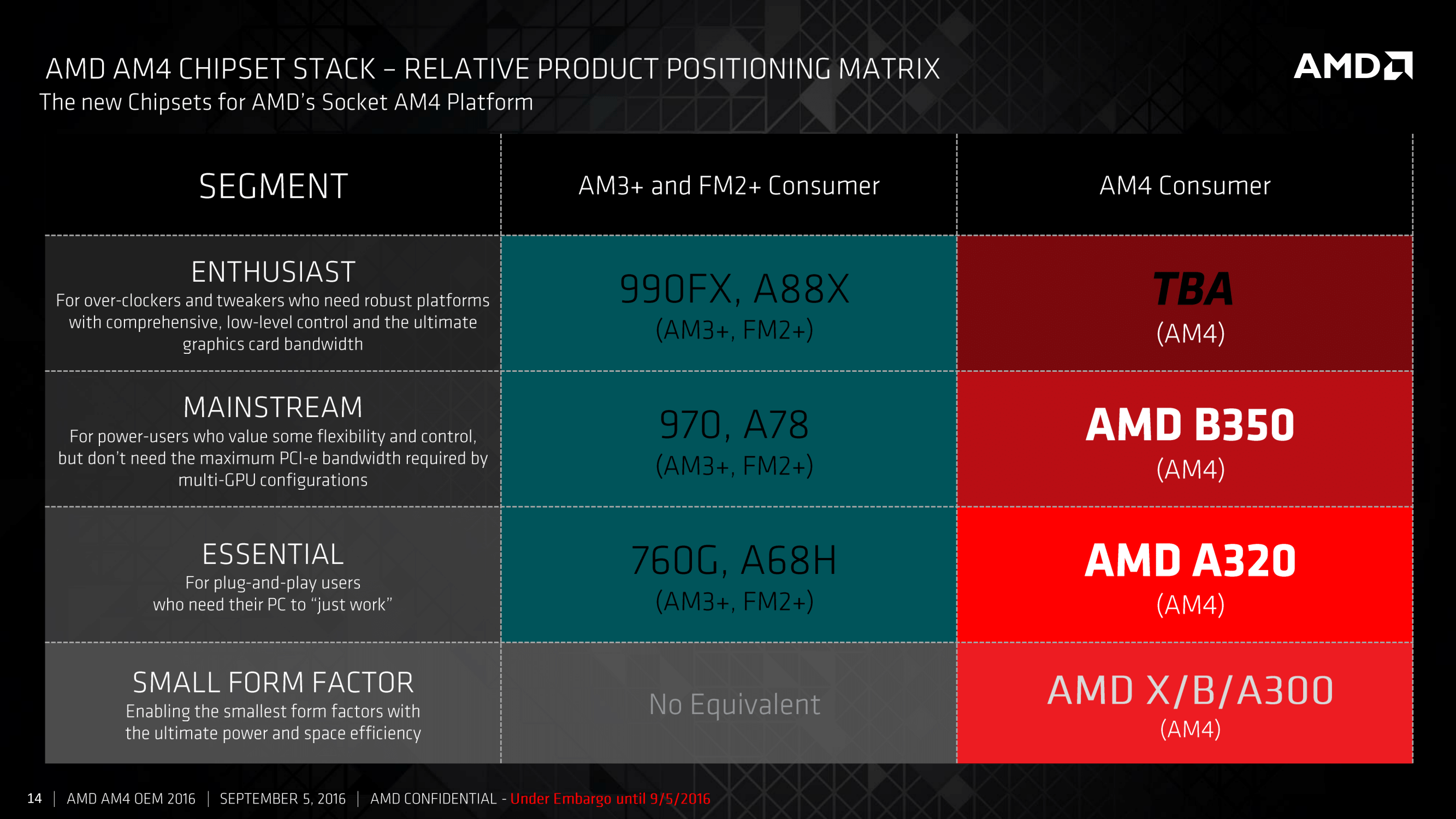
It’s worth noting that AMD has specifically listed that the B350 chipset is not the premium chipset for AM4. We know that Zen will be a part of the AM4 socket and ecosystem, and it would seem that there is at least one specific chipset for the high-end desktop market set to come later. Feel free to speculate.
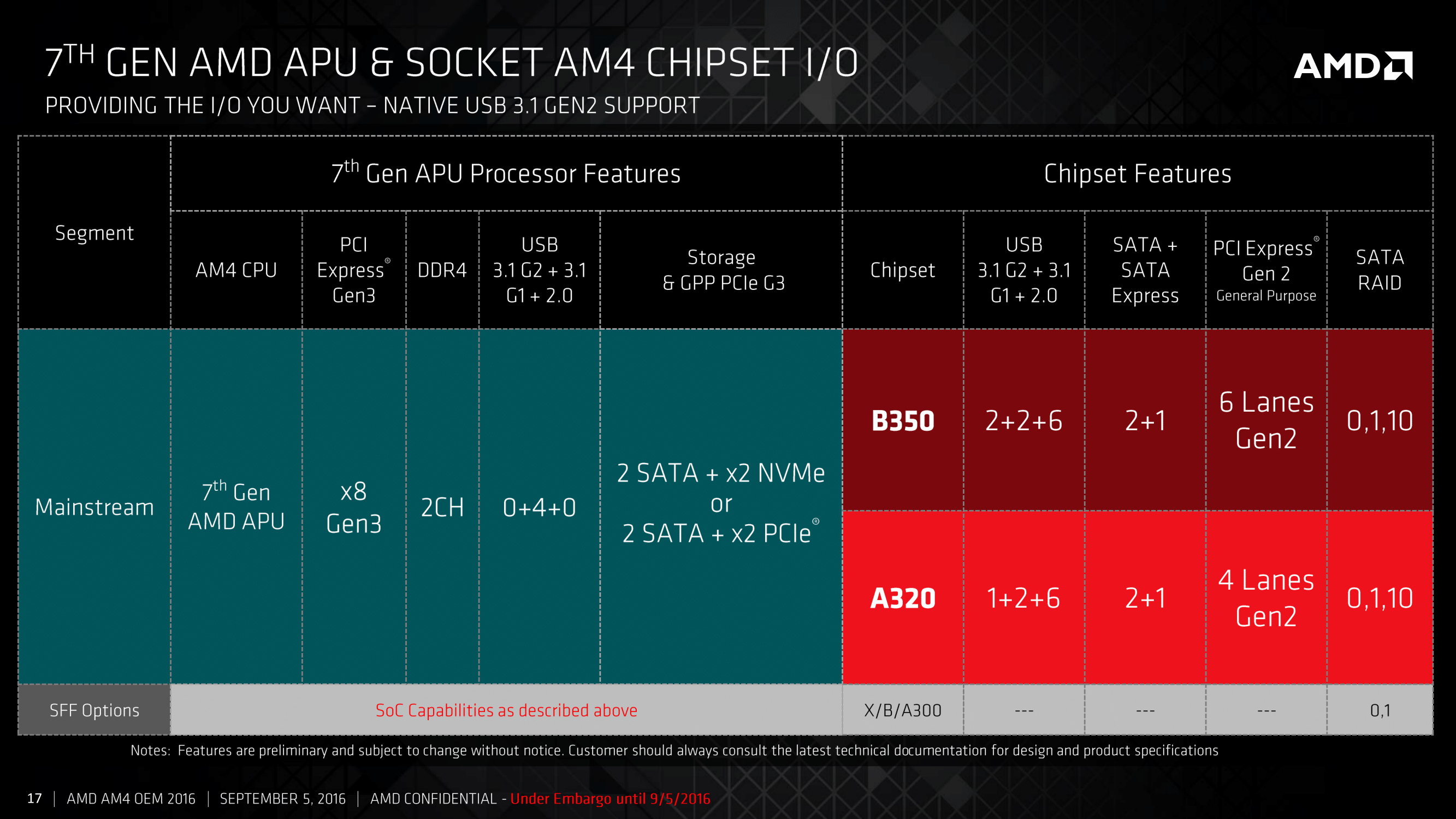
The B350 and A320 chipsets are mostly identical, using the PCIe 3.0 x4 from the CPU and offering a variety of SATA, USB and PCIe 2.0 connectivity. The PCIe 2.0 lanes, six on the B350 chipset and four on the A320 chipset, support x1, x2 and x4 modes for an array of different controllers. Perhaps the interesting thing here is the support of USB 3.1 at 10 Gbps, which is provided as native support from the chipset.
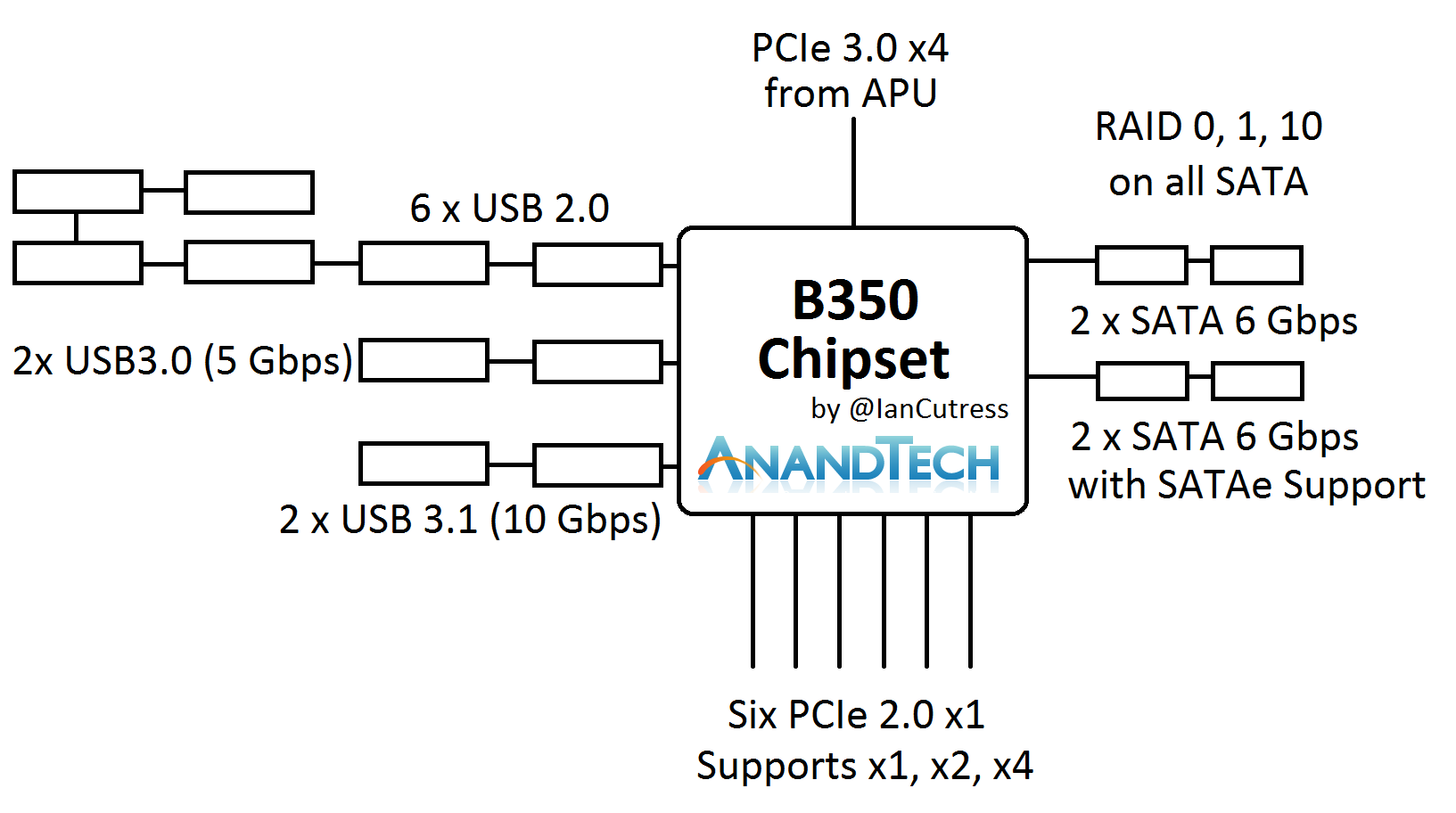
The main provider of USB 3.1 controllers in the market currently, ASMedia, has been floated around as a partner with AMD in designing these chipsets. We asked AMD if ASMedia was involved, and to what extent, in the development or IP of the hardware. We were told that while the IP is with AMD, ASMedia were bought on as a partner in some fashion (most likely as a design firm or a consultant) to help produce the hardware. We were informed that the chipsets are manufactured at TSMC using a 55nm process, which is a much cheaper process than 28nm or 16nm.
An additional aside, the chipset USB 3.1 ports do not support reversible Type-C natively. We have been informed that a re-driver chip is required to support the revisable connectivity, which is a minor additional IC required by the OEMs.
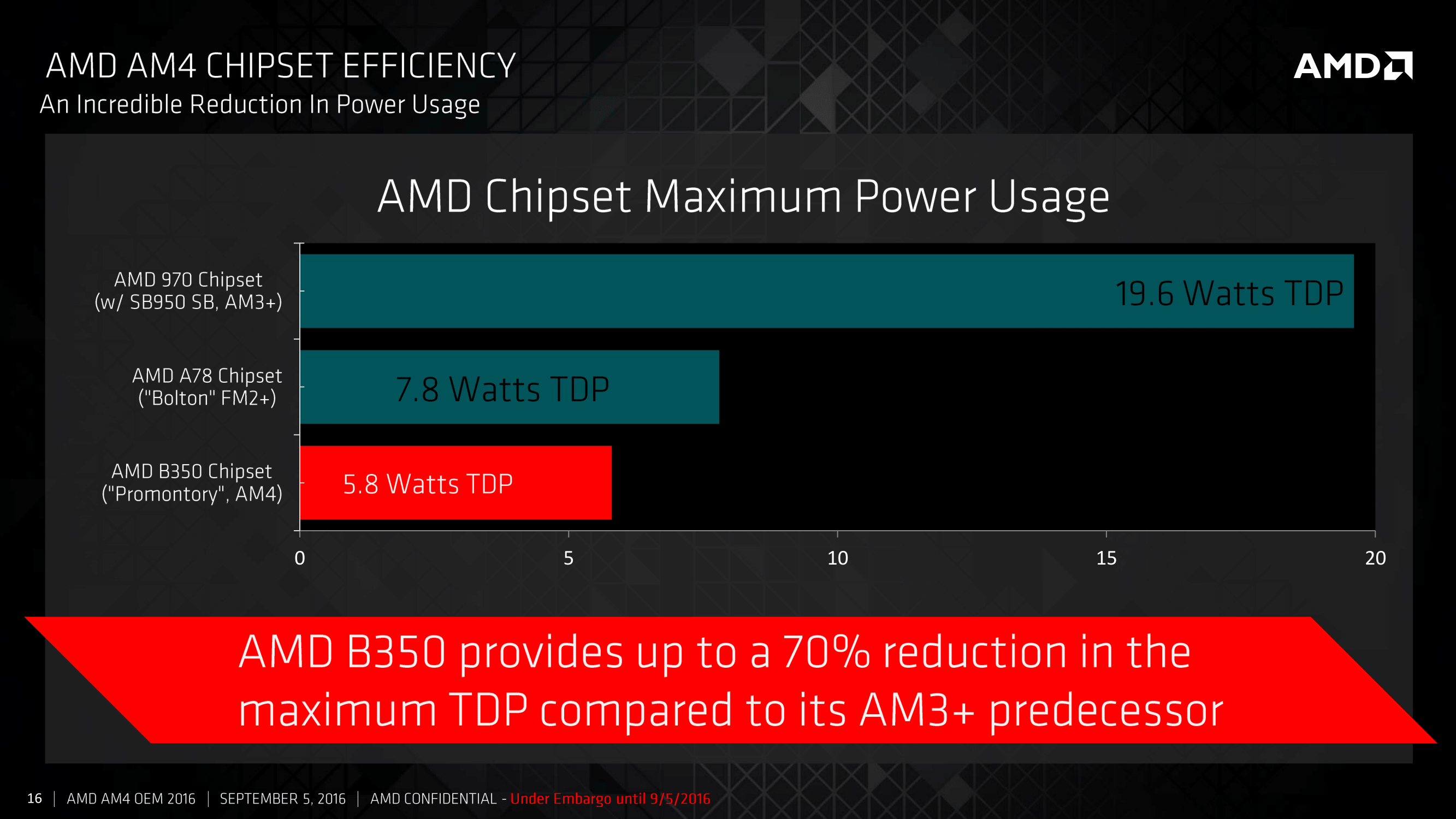
Aside from the native USB 3.1 output, AMD’s chipset offerings are far behind Intel’s current implementation, affording up to 20 PCIe 3.0 lanes from their chipset despite the same uplink equivalent. This is partly because Intel’s chipset has steadily grown and looks more like a PCIe switch itself. AMD is claiming that the external B350 chipset, compared to the older AM3 platforms, comes down from 19.6W TDP to 5.8W TDP.


122 Comments
View All Comments
DanNeely - Friday, September 23, 2016 - link
X = 1Y = 2
Z = 3
HL3 confirmed for 2017 launch.
anatol1981 - Friday, September 23, 2016 - link
Please, correct L1D info - its wrong.anatol1981 - Friday, September 23, 2016 - link
As i can see, L1-I swapped with L1-D, please, reverse them^)Mr Perfect - Friday, September 23, 2016 - link
Any chance the enthusiast grade chipset will be fabbed at the more expensive 28nm or 16nm node? Highend systems could justify the cost.Tom Womack - Friday, September 23, 2016 - link
The cost of fabbing a device at a different node is conservatively fifty million dollars; you're talking about a total reimplementation and revalidation, followed by a complete new mask set. There aren't half a million people willing to pay $100 more for an indifferent AMD chipset fabricated on a slightly shinier process.Mr Perfect - Friday, September 23, 2016 - link
That's assuming that the highend chipset was designed for the 55nm process from the start and would need to be redesigned for 28nm. If they designed the highend stuff for 28nm right from the start, it would just be fabrication cost differences.You're probably right though. They probably didn't see a big enough benefit in doing the C380(or whatever it ends up being called) at a modern node.
patrickjp93 - Tuesday, September 27, 2016 - link
Intel must be able to do it for far less, because there's no way Coffee Lake will sell that well, and it's based on the Cannonlake architecture which was originally built with 10nm in mind.Kalelovil - Sunday, September 25, 2016 - link
The desktop enthusiast market is unlikely to care for the couple of watts of power that could save.For the laptop market where power matters a lot more, I expect the Zen APU to integrate more connectivity onto the die and do away with the south-bridge entirely.
patrickjp93 - Tuesday, September 27, 2016 - link
Those are cheaper nodes due to maturity, jsyk.starlightmica - Friday, September 23, 2016 - link
HP Canada's 510-p127c spec page:http://support.hp.com/ca-en/document/c05281246
AMD A12-9000
16GB DDR4
R7 450 2Gb GDDR5, 4K over DP1.2, HDMI 1.4
180W uATX PSU :(