AMD 7th Gen Bristol Ridge and AM4 Analysis: Up to A12-9800, B350/A320 Chipset, OEMs first, PIBs Later
by Ian Cutress on September 23, 2016 9:00 AM ESTThe Two Main Chipsets: B350 and A320
Despite all the crazy potential that might come from playing with PCIe, if a user wants more than a couple of SATA ports or x1 slots, the chipset is there to provide. For the Bristol Ridge OEM launch, there are two main chipsets with a further three aimed more at embedded platforms. We’ll focus more on the first two.
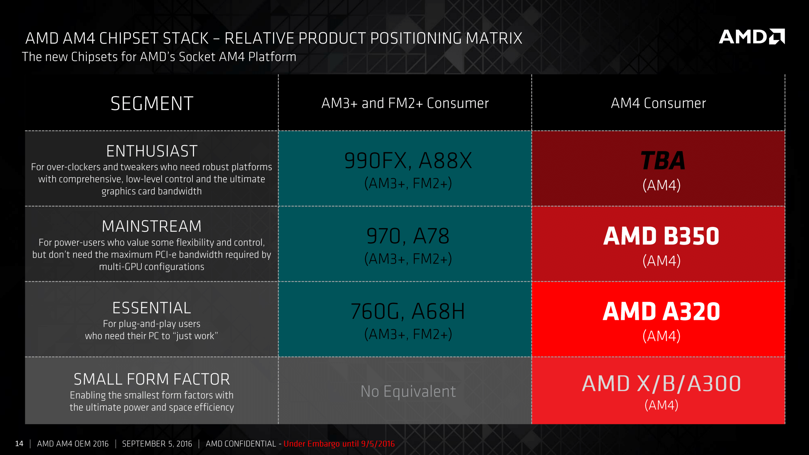
It’s worth noting that AMD has specifically listed that the B350 chipset is not the premium chipset for AM4. We know that Zen will be a part of the AM4 socket and ecosystem, and it would seem that there is at least one specific chipset for the high-end desktop market set to come later. Feel free to speculate.
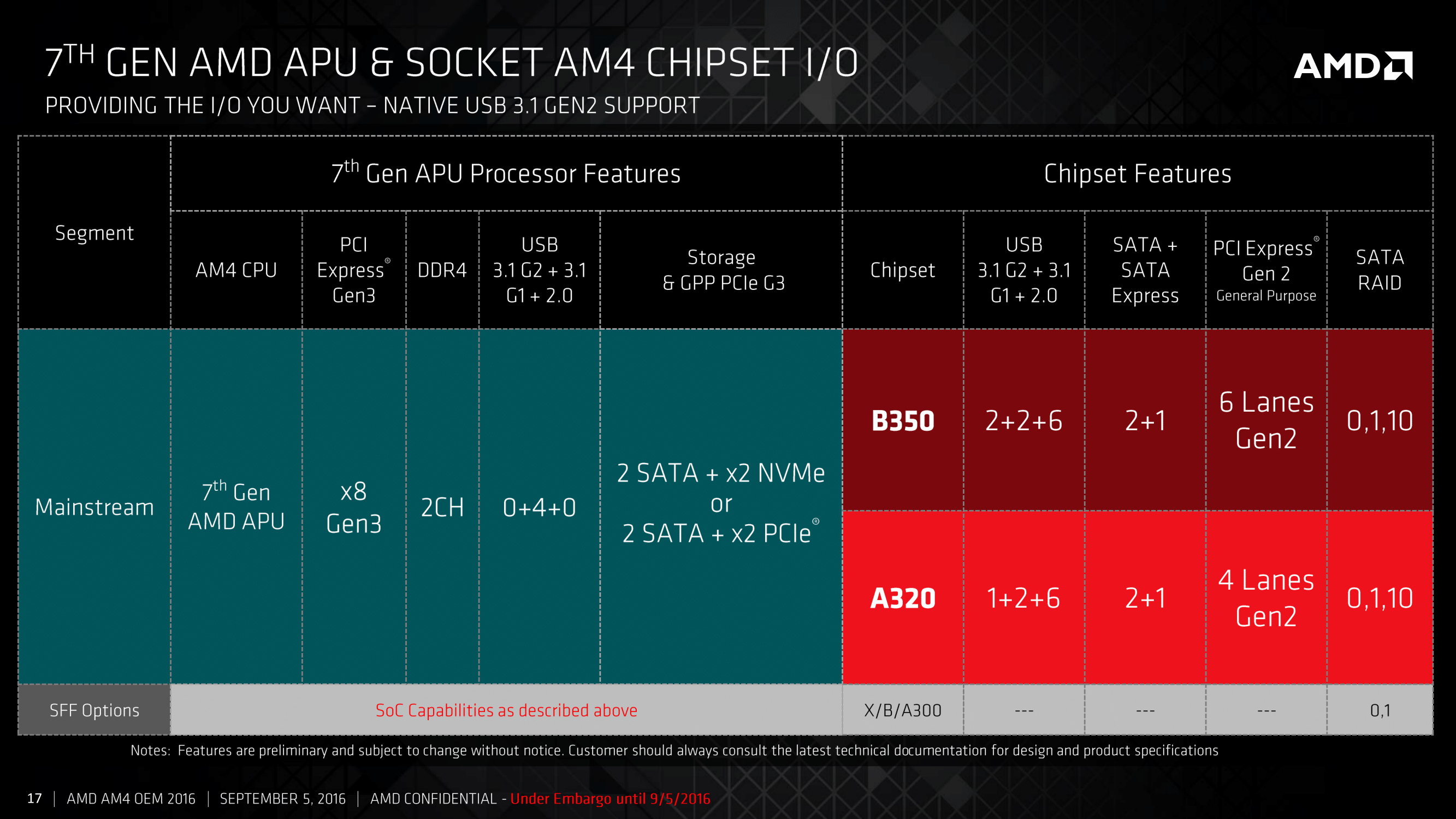
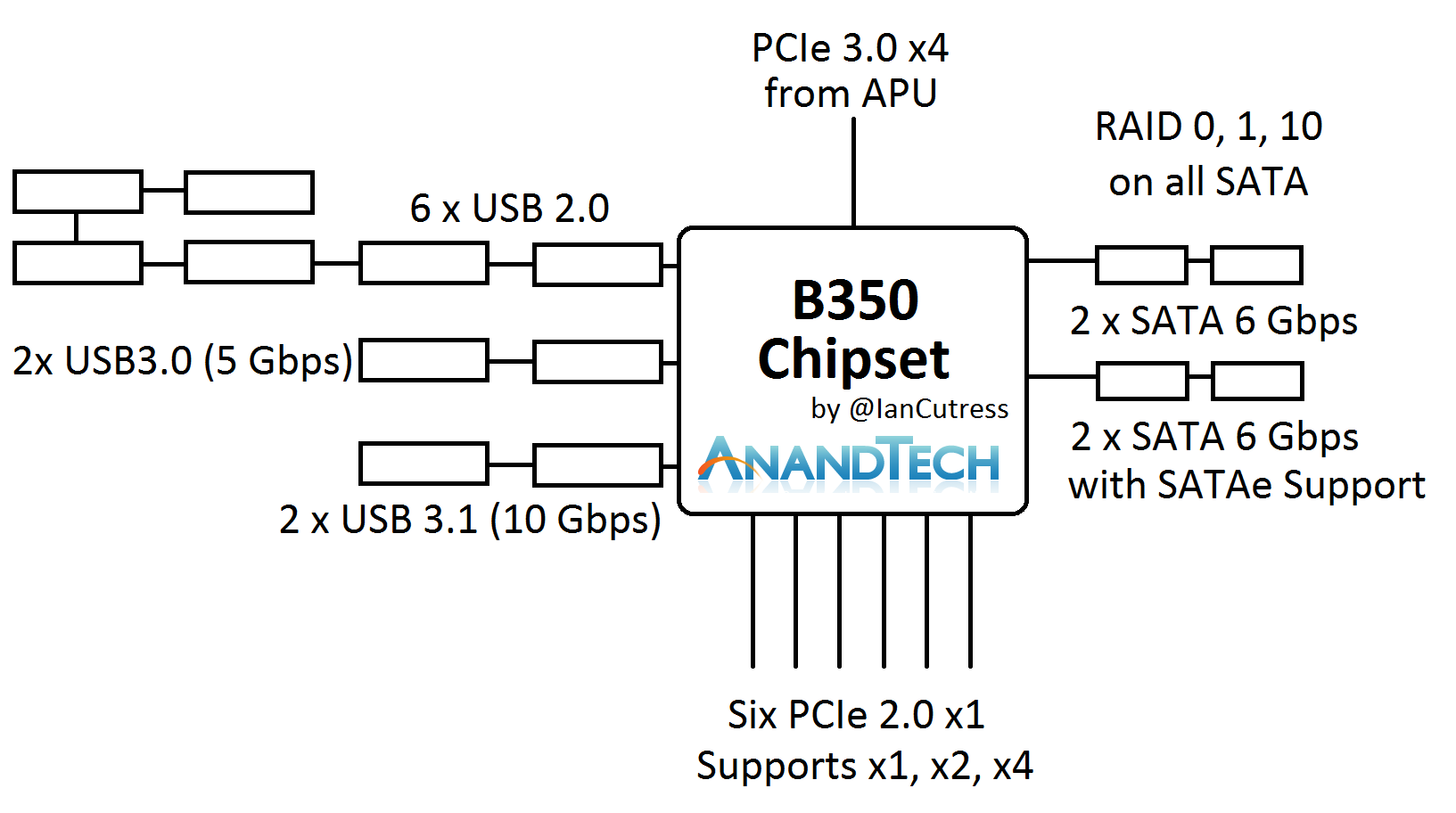
The B350 and A320 chipsets are mostly identical, using the PCIe 3.0 x4 from the CPU and offering a variety of SATA, USB and PCIe 2.0 connectivity. The PCIe 2.0 lanes, six on the B350 chipset and four on the A320 chipset, support x1, x2 and x4 modes for an array of different controllers. Perhaps the interesting thing here is the support of USB 3.1 at 10 Gbps, which is provided as native support from the chipset.
The main provider of USB 3.1 controllers in the market currently, ASMedia, has been floated around as a partner with AMD in designing these chipsets. We asked AMD if ASMedia was involved, and to what extent, in the development or IP of the hardware. We were told that while the IP is with AMD, ASMedia were bought on as a partner in some fashion (most likely as a design firm or a consultant) to help produce the hardware. We were informed that the chipsets are manufactured at TSMC using a 55nm process, which is a much cheaper process than 28nm or 16nm.
An additional aside, the chipset USB 3.1 ports do not support reversible Type-C natively. We have been informed that a re-driver chip is required to support the revisable connectivity, which is a minor additional IC required by the OEMs.
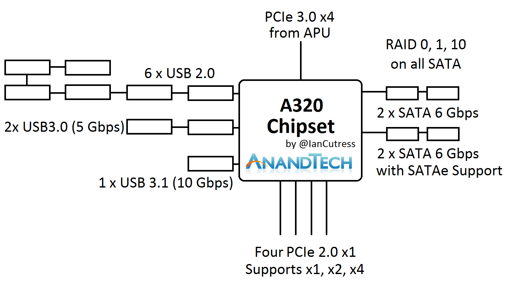
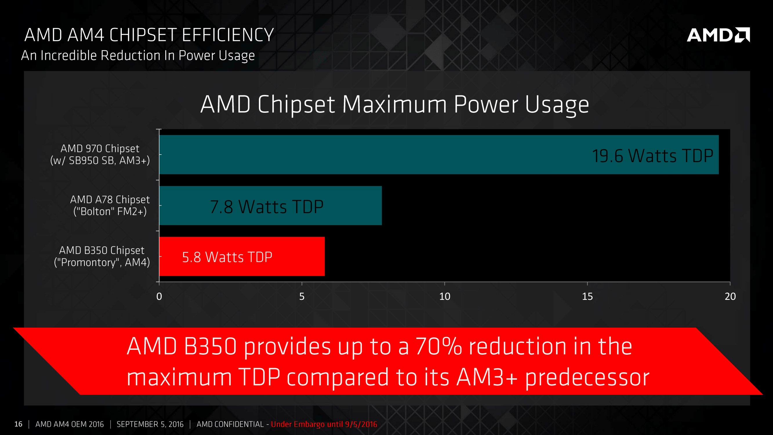
Aside from the native USB 3.1 output, AMD’s chipset offerings are far behind Intel’s current implementation, affording up to 20 PCIe 3.0 lanes from their chipset despite the same uplink equivalent. This is partly because Intel’s chipset has steadily grown and looks more like a PCIe switch itself. AMD is claiming that the external B350 chipset, compared to the older AM3 platforms, comes down from 19.6W TDP to 5.8W TDP.


122 Comments
View All Comments
patrickjp93 - Tuesday, September 27, 2016 - link
Yeah, no. Even the 5775C has thoroughly beaten everything AMD has so far offered, even if narrowly. Skylake GT3e increased that gap, and GT4e dug a canyon between Intel and AMD. This is why I sincerely doubt AMD's HPC APUs will get much traction.MrCommunistGen - Tuesday, September 27, 2016 - link
Skylake's GT4e really is in a whole new league of iGPU performance (at a significant cost) - but to nitpick GT3e on Skylake very likely underperforms GT3e on Broadwell.Broadwell GT3e (specifically Iris Pro 6200) is 48EUs at up to 1150MHz backed by 128MB eDRAM on a 65W TDP quad core.
Skylake GT3e (specifically Iris Graphics 550) is 48EUs at up to 1100MHz backed by 64MB eDRAM on a 28W dual core. (I'm not counting the listing for the "Server" GT3e which is listed as P555 with 128MB)
Skylake has microarchitecture improvements to both the EUs and to the x86 cores. It also supports DDR4 and Gen9 includes delta compression - so the iGPU undoubtedly has more bandwidth available.
That said, I really think that the smaller eDRAM, lower TDP, and lower max clock speed will make SKL GT3e slower than BDW GT3e.
Due to the rearrangement of SKUs and iGPUs in SKL I think this is all natural. Intel is trying to *significantly* increase the iGPU perf available to their 15/28W dual core CPUs with its iteration of GT3e, however this allows for the potential that this architecture's GT3e underperforms the previous.
Danvelopment - Saturday, September 24, 2016 - link
Something seems a bit funny about the IGPs of the A8 and A6. The A8 states R7 with 384SPs and a lower clock than the R5 in the A6 also with 384SPs.Should the A6 be R7 or 256 SPs? And if it's correct, how does the IGP compare between the two? And what makes the A8 faster?
Danvelopment - Saturday, September 24, 2016 - link
Also, any chance in getting a couple R5 performance indicators?MrCommunistGen - Tuesday, September 27, 2016 - link
I noticed that too. I've seen tables and slides from various sites and they all list those specs. The only thing I can conclude is that since the A6 has half the CPU resources, maybe AMD just assumes that for most tasks you'll end up CPU bound to a large enough degree that even thought the iGPU is technically faster, performance will be lower.Or... the alternative is that there's a typo of some sort in the original materials published by AMD.
yannigr2 - Saturday, September 24, 2016 - link
Oh, really nice article. Thanks for this.Well the first Zen processors will probably cost more than the A12. Then when Zen based APUs will be ready to come to the market, we will see and smaller Zen models.
ET - Saturday, September 24, 2016 - link
Thanks for the writeup, Ian. I even learned some new things which I haven't yet read elsewhere. I do hope that Anandtech can get its hands on a chip for reviews.NeatOman - Sunday, September 25, 2016 - link
Marginal improvement IMO over last gen APU's. Looks interesting but an i3 will still "feel" faster as its single core power is still greater, although i almost always build AMD APU's for small offices because Microcenter has a instant $40 rebate when you buy in store. BUT.. ZEN SoC with HBM might be a game changer (to quote 2014), and rumor is Apple is eyeballing it for the next Macbook Pro. And AMD has a good track record on Unix based OS's which might be why the Mac Pro uses AMD... I'm going down a rabbit hole. SOO! A12... ehh.. no significant change but I'm waiting for ZEN.utroz - Sunday, September 25, 2016 - link
Ian Cutress on the first page you say: "Using the updated 28nm process from TSMC, AMD was able to tweak the microarchitecture and allow full on APUs for desktops using a similar design."Problem is that Carrizo and Bristol Ridge are actually made at Global Foundries on a 28nm process.
TheinsanegamerN - Monday, September 26, 2016 - link
"Back at Computex, AMD announced the thing to fill that hole: Bristol Ridge (and Stoney Ridge by extension). This is what AMD will call and market it's '7th Generation' of APUs, and will be built on TSMC's 28nm Bulk CMOS process."From anandtech's look at carrizo in july. Everything else i've found doesnt say GF or TSMC, just 28nm.
so far, evidence is pointing at TSMC, not GF.