Assessing IBM's POWER8, Part 2: Server Applications on OpenPOWER
by Johan De Gelas on September 15, 2016 8:01 AM ESTFuture Visions, Cont: POWERed by NVIDIA
We have to check for ourselves of course, but IBM claims that compared to a dual K80 setup, a dual P100 gets a 2.07x speedup on the S822LC HPC. The same dual P100 on a fast Xeon with PCIe 3.0 only saw a 1.5x speedup. The benchmark used was a rather exotic Lattice QCD, or an approach to "solve quantum chromodynamics".
However, IBM reports that NVLink removes performance bottlenecks in
- FFT (signal processing)
- STAC-A2 (risk analysis)
- CPMD - computational chemistry
- Hash tables (used in many algorithms, security and big data)
- Spark
Those got our attention as, they are not some exotic niche HPC applications, but wide spread software components/frameworks used in both the HPC and data analytics world.
NVIDIA also claims that thanks to NVLink and the improved page migration engine capabilities, a new breed of GPU accelerated applications will be possible. The unified memory space (CUDA 6) introduced in Kepler was a huge step forward for the CUDA programmers: they no longer had to explicitly copy data from the CPU to the GPU. The Page Migration Engine would do that for them.
But the current system (Kepler and Maxwell) also had quite a few limitations. For example the memory space where the CPU and GPU are sharing data was limited to size of the GPU memory (typically 8-16 GB). The P100 now gets 49-bit virtual addressing, which means CUDA programs can thread every available RAM byte as one big virtual space. In the case of the newly launched S822LC, this means up to 1 TB of DRAM, and consequently 1 TB of memory space. Secondly, the whole virtual address space is coherent thanks to the new page fault mechanism: both the CPU and GPU can access the DRAM together. This requires OS support, and NVIDIA cooperated with the Linux community to make this happen.
Of course as the unified memory space gets larger, the amount of data to transfer back and forth gets larger too and that is where NVLink and the extra memory bandwidth of the POWER8 have a large advantage. Remember that even the POWER8 with only 4 buffer chips delivered twice as much memory bandwidth than the best Xeons. The higher end POWER8 have 8 buffer chips, and as a result offer almost twice as much memory bandwidth.
NVLink, together with the beefy memory subsystem of the POWER8, ensures that CUDA applications using such a unified 1TB memory space can actually work well.
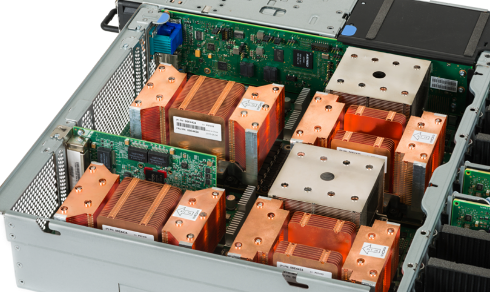
The POWER8 - al heatsinks - looks less hot headed now that it has the companion of 4 Tesla P100 GPUs...
The S822LC will cost less than $50000, and it offers a lot of FLOPS per dollar if you ask us. First consider that a single Tesla P100 SXM2 costs around $9500. The S822LC integrates four of them, two 10-core POWER8s and 256 GB of RAM. More than 21 TFLOPS (FP64) connected by the latest and greatest interconnects in a 2U box: the S822LC HPC is going to turn some heads.
Last but not least, note that once you add two or more GPUs which consume 300W each, the biggest disadvantage of the POWER8 almost literally melts away. The fact that each POWER8 CPU may consume 45-100W more than the high performance Xeons seems all of a sudden relative and not such a deal breaker anymore. Especially in the HPC world, where performance is more important than Watts.


49 Comments
View All Comments
JohanAnandtech - Sunday, September 25, 2016 - link
Thanks Jesper. Looks like I will have to spend even more time on that system :-). And indeed, out of the box performance is important if IBM ever wants to get a piece of the x86 market.luminarian - Thursday, September 15, 2016 - link
It was my understanding that the SMT mode on the power8 could be changed. Depending on the type of work this would make a giant difference, especially with mysql/mariadb that are limited to 1 process/thread per connection.With databases the real winner would be with one that supports parallel queries, such as postgresql 9.6, db2, oracle, etc.
Also yer bench mark very easily could be limiting the power8 if its not opening enough connections to fill out the number of threads that thing can handle, remember mysql/mariaDB are 1 process/thread per connection. Alot of database bench marks default to a small number of connections, this thing has 160 threads with the dual 10 core. I would suggest trying to run that same benchmark again but do it at the same time from multiple client machines. See if the bench takes a larger dip when a second client machine runs the same bench or if the bench shows similar figures(granted this might hit hd io limit on the power8 server).
So yea, that and try SMT-2 and SMT-4 modes.
JohanAnandtech - Friday, September 16, 2016 - link
Hi, I tried SMT-4, throughput was about 25% worse: 11k instead 14k+. 95th perc response time was better: 3.7 ms.JohanAnandtech - Friday, September 16, 2016 - link
updated the MySQL graphs with SMT-4 data. Our Spark tests gets worse with SMT-4 and that is also true for SPECjbb.luminarian - Friday, September 16, 2016 - link
Awesome, Thanks for the response.Meteor2 - Friday, September 16, 2016 - link
The HPC potential is awesome. You can really see why Oak Ridge chose POWER9 and Volta.Communism - Sunday, September 18, 2016 - link
Pretty sure most of the reason for that is due to Intel blocking every attempt Nvidia makes at getting a high bandwidth interface bolted onto a Xeon.Given that one of the main reasons that Intel blocked Nvidia's chipset business way back in the day was to try to limit the ability of other companies bolting on high bandwidth accelerators onto Intel chips (Presumably to protect their own initiatives in that space).
Klimax - Saturday, September 17, 2016 - link
Not terribly impressive. You have to get SW to paly nice and spend time to fine tune it to outperform Intel and it will cost you in power and cooling. More like "yes, if you get quite bigger TDP you get bit more power". And it won't be terribly good in many cases. (Like public facing service where latency is critical)Maybe if you are in USA and can waste admins and devs time and waste a lot on cooling and electricity then maybe. Otherwise why bother...
SarahKerrigan - Sunday, September 18, 2016 - link
I don't see this as a bad result. This is a 22nm processor, over two years old, and it beats Haswell-EP (which is newer) on efficiency. Broadwell-EP is brand new, and P9 should come out well before the end of BDW-EP's lifecycle.Kevin G - Sunday, September 18, 2016 - link
Some of the POWER9 chips will be out next year though is suspect that the scale-up models maybe an early 2018 part. Considering that those chips go into IBM's big iron Unix servers, they tend to launch a bit later than the low end models so it isn't game changing.The real question is when SkyLake-EP/EX will launch and in comparison to the scale-out POWER9 chips. I was expecting a first half of 2017 for the Intel parts but I have no reference as to when to expect the POWER9 SO chips. Thus there is a chance Intel can come out first.
Intel also wants a quick transition to SkyLake-EP/EX as they unify those to lines to some extent and provide some major platform improvements. I'm thinking Broadwell-EP/EX will have a relatively short life span compared to Haswell-EP/EX. This mimics much of what happened on the desktop and the challenge to move to 14 nm.