Ten Year Anniversary of Core 2 Duo and Conroe: Moore’s Law is Dead, Long Live Moore’s Law
by Ian Cutress on July 27, 2016 10:30 AM EST- Posted in
- CPUs
- Intel
- Core 2 Duo
- Conroe
- ITRS
- Nostalgia
- Time To Upgrade
Core: Decoding, and Two Goes Into One
The role of the decoder is to decipher the incoming instruction (opcode, addresses), and translate the 1-15 byte variable length instruction into a fixed-length RISC-like instruction that is easier to schedule and execute: a micro-op. The Core microarchitecture has four decoders – three simple and one complex. The simple decoder can translate instructions into single micro-ops, while the complex decoder can convert one instruction into four micro-ops (and long instructions are handled by a microcode sequencer). It’s worth noting that simple decoders are lower power and have a smaller die area to consider compared to complex decoders. This style of pre-fetch and decode occurs in all modern x86 designs, and by comparison AMD’s K8 design has three complex decoders.
The Core design came with two techniques to assist this part of the core. The first is macro-op fusion. When two common x86 instructions (or macro-ops) can be decoded together, they can be combined to increase throughput, and allows one micro-op to hold two instructions. The grand scheme of this is that four decoders can decode five instructions in one cycle.
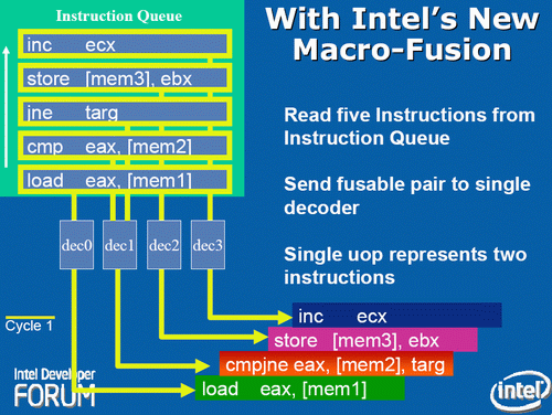
According to Intel at the time, for a typical x86 program, 20% of macro-ops can be fused in this way. Now that two instructions are held in one micro-op, further down the pipe this means there is more decode bandwidth for other instructions and less space taken in various buffers and the Out of Order (OoO) queue. Adjusting the pipeline such that 1-in-10 instructions are fused with another instruction should account for an 11% uptick in performance for Core. It’s worth noting that macro-op fusion (and macro-op caches) has become an integral part of Intel’s microarchitecture (and other x86 microarchitectures) as a result.
The second technique is a specific fusion of instructions related to memory addresses rather than registers. An instruction that requires an addition of a register to a memory address, according to RISC rules, would typically require three micro-ops:
| Pseudo-code | Instructions |
| read contents of memory to register2 | MOV EBX, [mem] |
| add register1 to register2 | ADD EBX, EAX |
| store result of register2 back to memory | MOV [mem], EBX |
However, since Banias (after Yonah) and subsequently in Core, the first two of these micro-ops can be fused. This is called micro-op fusion. The pre-decode stage recognizes that these macro-ops can be kept together by using smarter but larger circuitry without lowering the clock frequency. Again, op fusion helps in more ways than one – more throughput, less pressure on buffers, higher efficiency and better performance. Alongside this simple example of memory address addition, micro-op fusion can play heavily in SSE/SSE2 operations as well. This is primarily where Core had an advantage over AMD’s K8.
AMD’s definitions of macro-ops and micro-ops differ to that of Intel, which makes it a little confusing when comparing the two:
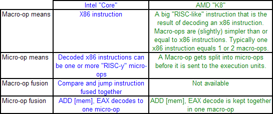
However, as mentioned above, AMD’s K8 has three complex decoders compared to Core’s 3 simple + 1 complex decoder arrangement. We also mentioned that simple decoders are smaller, use less power, and spit out one Intel micro-op per incoming variable length instruction. AMD K8 decoders on the other hand are dual purpose: it can implement Direct Path decoding, which is kind of like Intel’s simple decoder, or Vector decoding, which is kind of like Intel’s complex decoder. In almost all circumstances, the Direct Path is preferred as it produces fewer ops, and it turns out most instructions go down the Direct Path anyway, including floating point and SSE instructions in K8, resulting in fewer instructions over K7.
While extremely powerful in what they do, AMD’s limitation for K8, compared to Intel’s Core, is two-fold. AMD cannot perform Intel’s version of macro-op fusion, and so where Intel can pack one fused instruction to increase decode throughput such as the load and execute operations in SSE, AMD has to rely on two instructions. The next factor is that by virtue of having more decoders (4 vs 3), Intel can decode more per cycle, which expands with macro-op fusion – where Intel can decode five instructions per cycle, AMD is limited to just three.
As Johan pointed out in the original article, this makes it hard for AMD’s K8 to have had an advantage here. It would require three instructions to be fetched for the complex decoder on Intel, but not kick in the microcode sequencer. Since the most frequent x86 instructions map to one Intel micro-op, this situation is pretty unlikely.


158 Comments
View All Comments
Akrovah - Wednesday, July 27, 2016 - link
My old E6700 is still alive and kicking. I only just replaced it as my primary system when Devil's Canyon came along. Still use it for my four year old's "first computer."djayjp - Wednesday, July 27, 2016 - link
Not a particle physicist, nor electrical engineer, so just some pie in the sky wondering here, but wouldn't it be possible to build transistors using carbon nanotubes, or light itself (using nano sized mirrors/interferometers, like DLP) or even basing the transistor gates off of protons/sub atomic particles?michael2k - Wednesday, July 27, 2016 - link
I think a more interesting question is using glass as a substrate. Imagine printing nand, CPU, GPU, ram, and along the bezels of a smartphone.That reduces a phone to six components: a display, a transducer for sound, a mic, a battery, a radio, and a chassis, which would have all the antennas.
joex4444 - Wednesday, July 27, 2016 - link
Particle physicist here. Light has the tricky property that it travels at the speed of light so I can't imagine it working but perhaps I'm envisioning your concept differently than you are. For carbon nanotubes, you'll need a materials engineer or a condensed matter physicist.3DoubleD - Wednesday, July 27, 2016 - link
Materials/Semiconductor Physics Engineer here. The problem is not what we CAN do, the problem is what is economically possible at scale. For example, FinFETs were demonstrated at the turn of the century, but took all of those years to become (1) necessary - planar transistor were getting too leaky, and (2) possible to fabricate economically in large scales.Researchers have created smaller, faster transistors years ago, but it takes a lot of time and effort to develop the EUV or quadruple patterning technologies that enable these devices to be reliably and affordably manufactured.
So I think the problem in moving "beyond silicon" is not that we don't have alternatives, it is that we have many alternatives, we just don't know which will scale. It becomes less of a purely engineering problem and manufacturing business problem. When new technologies relied purely on the established silicon industry alone, you could reasonably extrapolate how much each new technology would cost as the nodes were scaled down. When we talk about using III-V FinFETs/ All Around Gates or graphene and carbon nanotubes, we don't really know how those things will scale with the existing processes as we move them from the laboratory to the manufacturing line.
I've been looking forward to this transition for years. People moan that it is the end of Moores Law, but that could be a good thing. Silicon is a great material for forming logic circuits for many reasons, but it also has many downsides. While silicon never reached 10 GHz (as Intel once predicted), other materials easily blow past 100 GHz transistor switching speeds. When the massive engines that work tirelessly to reduce our lithography nodes nm by nm are aimed at "the next big thing", we might be pleasantly surprised by a whole new paradigm of performance.
So what competes with modern day Si CMOS on speed, power usage, and cost? Nothing... yet!
djayjp - Thursday, July 28, 2016 - link
Yes, it's fascinating stuff. Thanks for reminding me about that. I recall now that I think it was graphene that enabled those insanely high switching speeds, due to its incredible conductivity/efficiency. Hopefully it can now be made economically feasible at some point! Imagine a the next GPU that is 10x smaller and operates at 100x the clock speed. A GTX 1080Ti x 1000! Finally we can do real time true global illumination ha....jeffry - Monday, August 1, 2016 - link
Thats a good point. Like, answering a question "are you willing to pay $800 for a new CPU to double the computers speed?" Most consumers say no. It all comes down to the mass market price.wumpus - Thursday, August 4, 2016 - link
From the birth of the Univac until 10 years ago, consumers consistently said YES! and plunked down their money. Doubling the (per thread) speed of a core2duo is going to cost more than $800. Also the cost of the RAM on servers is *WAY* more than $800, so you can expect if Intel could double the power of each core, they could crank prices up by at least $800 per core on Xeons. They can't, and neither can IBM or AMD.Jaybus - Thursday, July 28, 2016 - link
Sure, but that speed is dependent on the medium. There are some proposed optical transistors using electromagnetically induced transparency. Long way off. However, silicon photonics could change some things. Capacitance is the killer for electronic interconnects, whether chip-to-chip or on-chip bus. An optical interconnect could greatly increase bandwidth without increasing the chip's power dissipation. I think an electronic-photonic hybrid is more likely, since silicon photonics components can be made on a CMOS process. We are already beginning to see optical PCI Express being deployed. I could definitely see a 3D approach where 2D electronic layers are connected through an optical rather than electronic bus.djayjp - Thursday, July 28, 2016 - link
Yes, transparency, like polarized windows that either become transparent or opaque when a current is applied (to the liquid crystals?). I wonder how small they could be made. It would be incredibly power efficient I would think.