Ten Year Anniversary of Core 2 Duo and Conroe: Moore’s Law is Dead, Long Live Moore’s Law
by Ian Cutress on July 27, 2016 10:30 AM EST- Posted in
- CPUs
- Intel
- Core 2 Duo
- Conroe
- ITRS
- Nostalgia
- Time To Upgrade
Core: Decoding, and Two Goes Into One
The role of the decoder is to decipher the incoming instruction (opcode, addresses), and translate the 1-15 byte variable length instruction into a fixed-length RISC-like instruction that is easier to schedule and execute: a micro-op. The Core microarchitecture has four decoders – three simple and one complex. The simple decoder can translate instructions into single micro-ops, while the complex decoder can convert one instruction into four micro-ops (and long instructions are handled by a microcode sequencer). It’s worth noting that simple decoders are lower power and have a smaller die area to consider compared to complex decoders. This style of pre-fetch and decode occurs in all modern x86 designs, and by comparison AMD’s K8 design has three complex decoders.
The Core design came with two techniques to assist this part of the core. The first is macro-op fusion. When two common x86 instructions (or macro-ops) can be decoded together, they can be combined to increase throughput, and allows one micro-op to hold two instructions. The grand scheme of this is that four decoders can decode five instructions in one cycle.
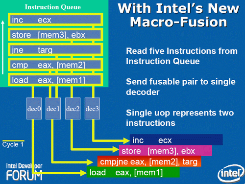
According to Intel at the time, for a typical x86 program, 20% of macro-ops can be fused in this way. Now that two instructions are held in one micro-op, further down the pipe this means there is more decode bandwidth for other instructions and less space taken in various buffers and the Out of Order (OoO) queue. Adjusting the pipeline such that 1-in-10 instructions are fused with another instruction should account for an 11% uptick in performance for Core. It’s worth noting that macro-op fusion (and macro-op caches) has become an integral part of Intel’s microarchitecture (and other x86 microarchitectures) as a result.
The second technique is a specific fusion of instructions related to memory addresses rather than registers. An instruction that requires an addition of a register to a memory address, according to RISC rules, would typically require three micro-ops:
| Pseudo-code | Instructions |
| read contents of memory to register2 | MOV EBX, [mem] |
| add register1 to register2 | ADD EBX, EAX |
| store result of register2 back to memory | MOV [mem], EBX |
However, since Banias (after Yonah) and subsequently in Core, the first two of these micro-ops can be fused. This is called micro-op fusion. The pre-decode stage recognizes that these macro-ops can be kept together by using smarter but larger circuitry without lowering the clock frequency. Again, op fusion helps in more ways than one – more throughput, less pressure on buffers, higher efficiency and better performance. Alongside this simple example of memory address addition, micro-op fusion can play heavily in SSE/SSE2 operations as well. This is primarily where Core had an advantage over AMD’s K8.
AMD’s definitions of macro-ops and micro-ops differ to that of Intel, which makes it a little confusing when comparing the two:
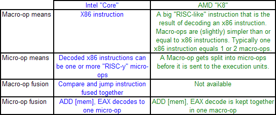
However, as mentioned above, AMD’s K8 has three complex decoders compared to Core’s 3 simple + 1 complex decoder arrangement. We also mentioned that simple decoders are smaller, use less power, and spit out one Intel micro-op per incoming variable length instruction. AMD K8 decoders on the other hand are dual purpose: it can implement Direct Path decoding, which is kind of like Intel’s simple decoder, or Vector decoding, which is kind of like Intel’s complex decoder. In almost all circumstances, the Direct Path is preferred as it produces fewer ops, and it turns out most instructions go down the Direct Path anyway, including floating point and SSE instructions in K8, resulting in fewer instructions over K7.
While extremely powerful in what they do, AMD’s limitation for K8, compared to Intel’s Core, is two-fold. AMD cannot perform Intel’s version of macro-op fusion, and so where Intel can pack one fused instruction to increase decode throughput such as the load and execute operations in SSE, AMD has to rely on two instructions. The next factor is that by virtue of having more decoders (4 vs 3), Intel can decode more per cycle, which expands with macro-op fusion – where Intel can decode five instructions per cycle, AMD is limited to just three.
As Johan pointed out in the original article, this makes it hard for AMD’s K8 to have had an advantage here. It would require three instructions to be fetched for the complex decoder on Intel, but not kick in the microcode sequencer. Since the most frequent x86 instructions map to one Intel micro-op, this situation is pretty unlikely.


158 Comments
View All Comments
Jon Tseng - Wednesday, July 27, 2016 - link
Great chip. Only just upgraded from my QX6850 last month. Paired with a GTX 970 it was doing just fine running all new games maxed out at 1080p. Amazing for something nearly a decade old!!Negative Decibel - Wednesday, July 27, 2016 - link
my E6600 is still kicking.tarqsharq - Wednesday, July 27, 2016 - link
My dad still uses my old E8400 for his main PC. He's getting my old i7-875k soon though.jjj - Wednesday, July 27, 2016 - link
You can't do DRAM in glasses, not in a real way. Since that's what mobile is by 2025.On-package DRAM is next year or soon not 2025.
You can't have big cores either and you need ridiculous GPUs and extreme efficiency. Parallelism and accelerators, that's where computing needs to go, from mobile to server.
We need 10-20 mm3 chips not 100cm2 boards. New NV memories not DRAM and so on.
Will be interesting to see who goes 3D first with logic on logic and then who goes 3D first as the default in the most advanced process.
At the end of the day, even if the shrinking doesn't stop, 2D just can't offer enough for the next form factor. Much higher efficiency is needed and the size of a planar chip would be far too big to fit in the device while the costs would be mad.Much more is needed. For robots too.The costs and efficiency need to scale and with planar it's at best little.
wumpus - Thursday, August 4, 2016 - link
On package DRAM seems to be a "forever coming" tech. AMD Fury-X basically shipped it, and it went nowhere. I'm guessing it will be used whenever Intel or IBM feel it can be used for serious advantage on some high-core server chip, or possibly when Intel want to build a high-speed DRAM cache (with high-speed-bus) and use 3dXpoint for "main memory".The slow rollout is shocking. I'm guessing nvidia eventually gave up with it and went with tiling (see the Kanter demo on left, but ignore the thread: nothing but fanboys beating their chests).
willis936 - Wednesday, July 27, 2016 - link
I'm certainly no silicon R&D expert but I'm very skeptical of those projections.Mr.Goodcat - Wednesday, July 27, 2016 - link
Typo:"On the later, we get the prediction that 450nm wafers should be in play at around 2021 for DRAM"
450nm wafers would be truly interesting ;-)
wumpus - Thursday, August 4, 2016 - link
I like the rapidly falling static safety. Don't breathe on a 2030 chip.faizoff - Wednesday, July 27, 2016 - link
My first Core 2 Duo was an E4400 that I bought in 2007 I believe, thing lasted me up to 2011 when I upgraded to an i5 2500k. I should've kept that C2D just for nostalgia's sake, I used it intermittently as a plex server and that thing worked great on FreeNAS. The only issue was it was really noisy and would get hot.Notmyusualid - Thursday, July 28, 2016 - link
I've got a few old servers kicking around, all with valid Win server licenses, but due to UK electricity costs, just can't bring myself to have them running at home 24/7 just to serve a backup, or yet another Breaking Bad viewing session... :) which we can do locally now.