The AMD Radeon RX 480 Preview: Polaris Makes Its Mainstream Mark
by Ryan Smith on June 29, 2016 9:00 AM ESTThe Polaris Architecture: In Brief
For today’s preview I’m going to quickly hit the highlights of the Polaris architecture.
In their announcement of the architecture this year, AMD laid out a basic overview of what components of the GPU would see major updates with Polaris. Polaris is not a complete overhaul of past AMD designs, but AMD has combined targeted performance upgrades with a chip-wide energy efficiency upgrade. As a result Polaris is a mix of old and new, and a lot more efficient in the process.
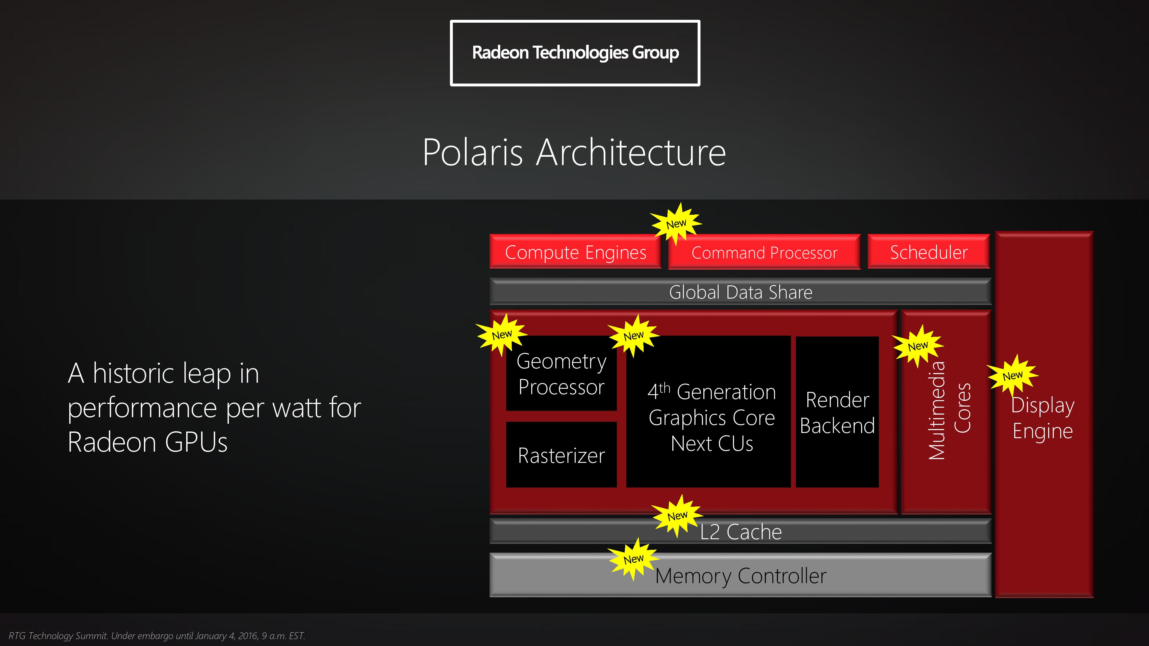
At its heart, Polaris is based on AMD’s 4th generation Graphics Core Next architecture (GCN 4). GCN 4 is not significantly different than GCN 1.2 (Tonga/Fiji), and in fact GCN 4’s ISA is identical to that of GCN 1.2’s. So everything we see here today comes not from broad, architectural changes, but from low-level microarchitectural changes that improve how instructions execute under the hood.
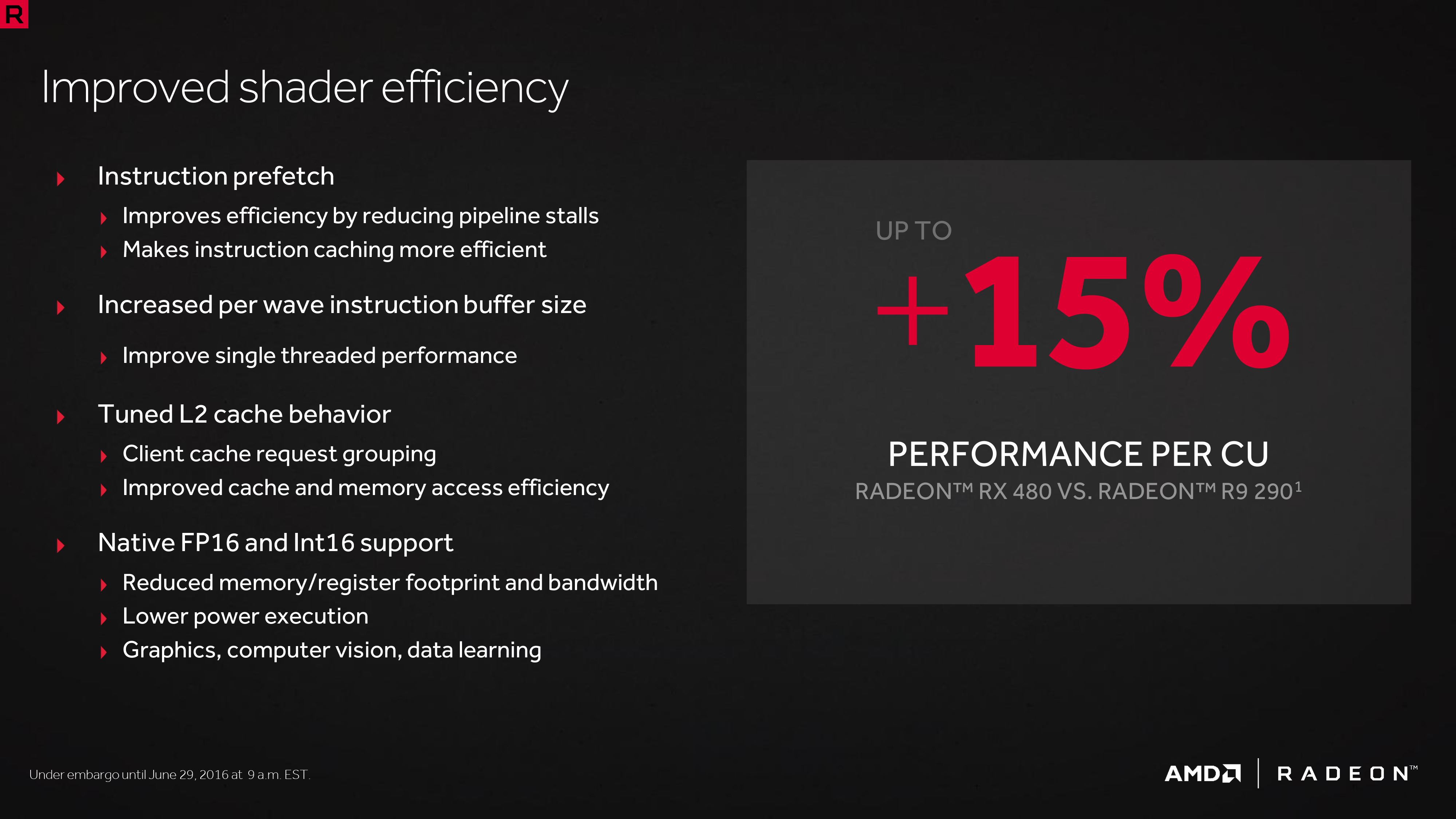
Overall AMD is claiming that GCN 4 (via RX 480) offers a 15% improvement in shader efficiency over GCN 1.1 (R9 290). This comes from two changes; instruction prefetching and a larger instruction buffer. In the case of the former, GCN 4 can, with the driver’s assistance, attempt to pre-fetch future instructions, something GCN 1.x could not do. When done correctly, this reduces/eliminates the need for a wave to stall to wait on an instruction fetch, keeping the CU fed and active more often. Meanwhile the per-wave instruction buffer (which is separate from the register file) has been increased from 12 DWORDs to 16 DWORDs, allowing more instructions to be buffered and, according to AMD, improving single-threaded performance.
Outside of the shader cores themselves, AMD has also made enhancements to the graphics front-end for Polaris. AMD’s latest architecture integrates what AMD calls a Primative Discard Accelerator. True to its name, the job of the discard accelerator is to remove (cull) triangles that are too small to be used, and to do so early enough in the rendering pipeline that the rest of the GPU is spared from having to deal with these unnecessary triangles. Degenerate triangles are culled before they even hit the vertex shader, while small triangles culled a bit later, after the vertex shader but before they hit the rasterizer. There’s no visual quality impact to this (only triangles that can’t be seen/rendered are culled), and as claimed by AMD, the benefits of the discard accelerator increase with MSAA levels, as MSAA otherwise exacerbates the small triangle problem.
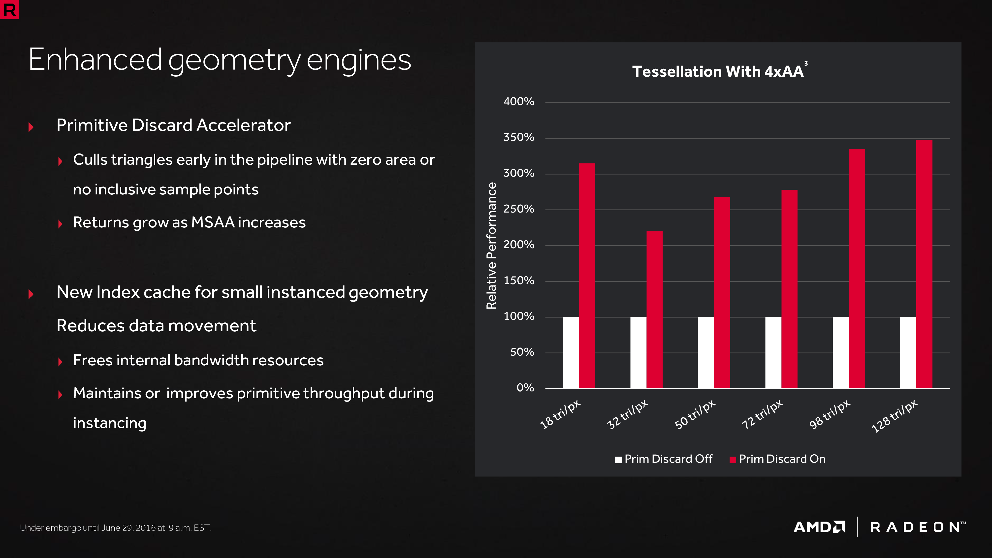
Along these lines, Polaris also implements a new index cache, again meant to improve geometry performance. The index cache is designed specifically to accelerate geometry instancing performance, allowing small instanced geometry to stay close by in the cache, avoiding the power and bandwidth costs of shuffling this data around to other caches and VRAM.
Finally, at the back-end of the GPU, the ROP/L2/Memory controller partitions have also received their own updates. Chief among these is that Polaris implements the next generation of AMD’s delta color compression technology, which uses pattern matching to reduce the size and resulting memory bandwidth needs of frame buffers and render targets. As a result of this compression, color compression results in a de facto increase in available memory bandwidth and decrease in power consumption, at least so long as buffer is compressible. With Polaris, AMD supports a larger pattern library to better compress more buffers more often, improving on GCN 1.2 color compression by around 17%.
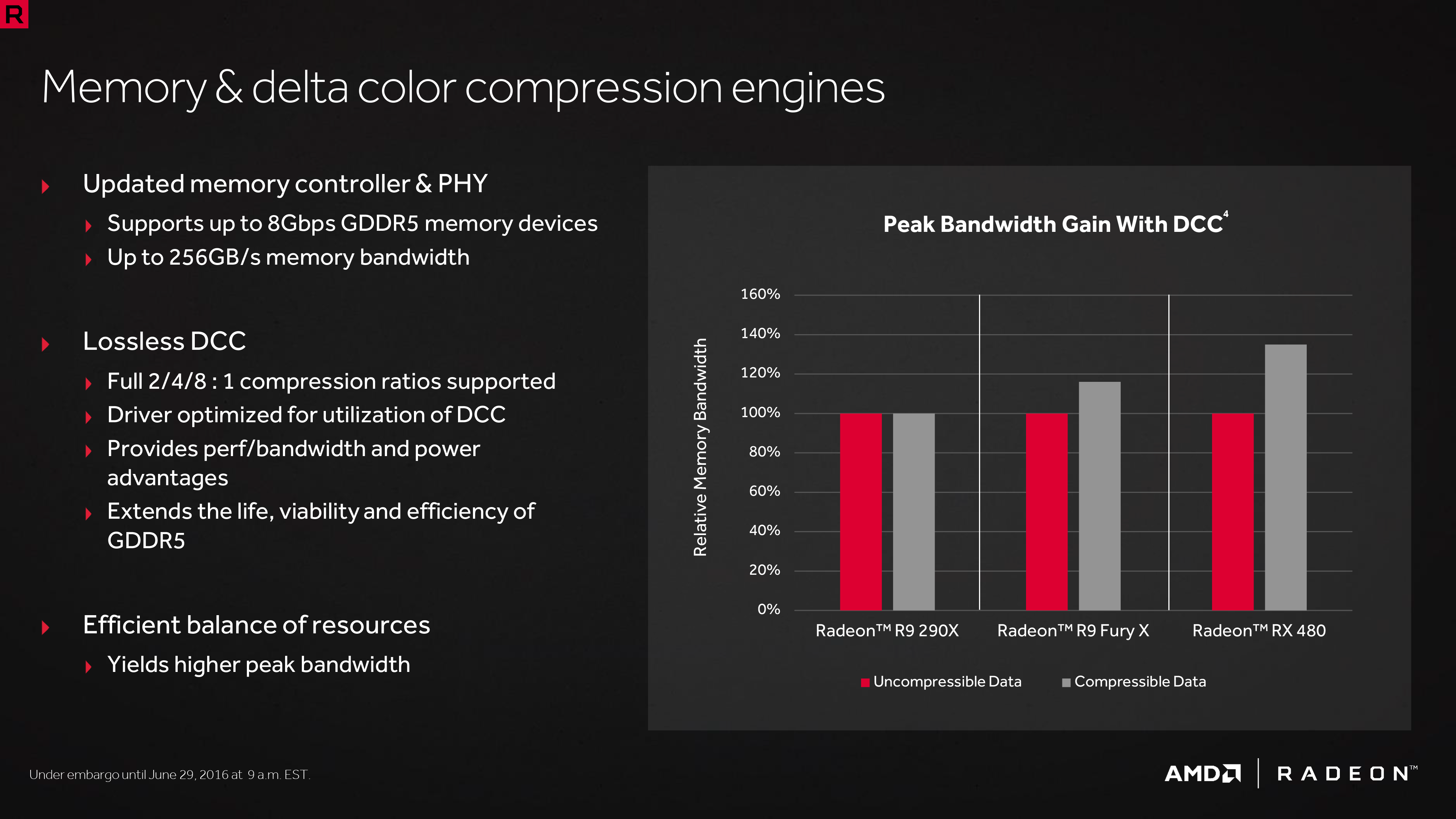
Otherwise we’ve already covered the increased L2 cache size, which is now at 2MB. Paired with this is AMD’s latest generation memory controller, which can now officially go to 8Gbps, and even a bit more than that when oveclocking.


449 Comments
View All Comments
FriendlyUser - Wednesday, June 29, 2016 - link
I don't think nVidia wants to compete on price. They'll probably present something equivalent or even marginally (5%) better so that they can "win" then sell it at a significantly higher price point. The price range from $239 to the $400+ of the 1070 has no next-generation products. I'm guessing something will quickly populate the $300-320 price point. Could be wrong, but would make more sense than going to $150.cocochanel - Thursday, June 30, 2016 - link
I doubt Nvidia can match this card. If they come up with one, they'll have to sell it at a loss.sonicmerlin - Friday, July 1, 2016 - link
You think Nvidia can't match their 2 year old 970 with 2 node jumps?Sushisamurai - Friday, July 1, 2016 - link
Thats a good point, I don't think they'll be able to match it, as there's a large R&D cost for developing a new chip and board on process jumps. The fact AMD can recuperate those costs @$200/240 is pretty nutsQuestor - Wednesday, June 29, 2016 - link
Amazing thought comparison to a card that doesn't exist yet. You must be in touch with your inner god.HollyDOL - Wednesday, June 29, 2016 - link
Well, maybe if you actually read what I wrote before you started seeing red, you would notice word LIKELY :praazman - Wednesday, June 29, 2016 - link
Don't worry, it's coming.fuicharles - Wednesday, June 29, 2016 - link
Provided there is stock available.HollyDOL - Wednesday, June 29, 2016 - link
hehe, touche :-)dragonsqrrl - Wednesday, June 29, 2016 - link
I doubt the 1060 will "have it for breakfast", but based on these results I now have little doubt that a card based on a fully enabled GP106 will be performance competitive with the RX480. Rumors and leaks prior to launch suggested that RX480 would trade blows with the 390X, which made me think the 1060 would probably perform a step below it.