The NVIDIA GeForce GTX 1080 & GTX 1070 Founders Editions Review: Kicking Off the FinFET Generation
by Ryan Smith on July 20, 2016 8:45 AM ESTDesigning GP104: Running Up the Clocks
So if GP104’s per-unit throughput is identical to GM204, and the SM count has only been increased from 2048 to 2560 (25%), then what makes GTX 1080 60-70% faster than GTX 980? The answer there is that instead of vastly increasing the number of functional units for GP104 or increasing per-unit throughput, NVIDIA has instead opted to significantly raise the GPU clockspeed. And this in turn goes back to the earlier discussion on TSMC’s 16nm FinFET process.
With every advancement in fab technology, chip designers have been able to increase their clockspeeds thanks to the basic physics at play. However because TSMC’s 16nm node adds FinFETs for the first time, it’s extra special. What’s happening here is a confluence of multiple factors, but at the most basic level the introduction of FinFETs means that the entire voltage/frequency curve gets shifted. The reduced leakage and overall “stronger” FinFET transistors can run at higher clockspeeds at lower voltages, allowing for higher overall clockspeeds at the same (or similar) power consumption. We see this effect to some degree with every node shift, but it’s especially potent when making the shift from planar to FinFET, as has been the case for the jump from 28nm to 16nm.
Given the already significant one-off benefits of such a large jump in the voltage/frequency curve, for Pascal NVIDIA has decided to fully embrace the idea and run up the clocks as much as is reasonably possible. At an architectural level this meant going through the design to identify bottlenecks in the critical paths – logic sections that couldn’t run at as high a frequency as NVIDIA would have liked – and reworking them to operate at higher frequencies. As GPUs typically (and still are) relatively low clocked, there’s not as much of a need to optimize critical paths in this matter, but with NVIDIA’s loftier clockspeed goals for Pascal, this changed things.
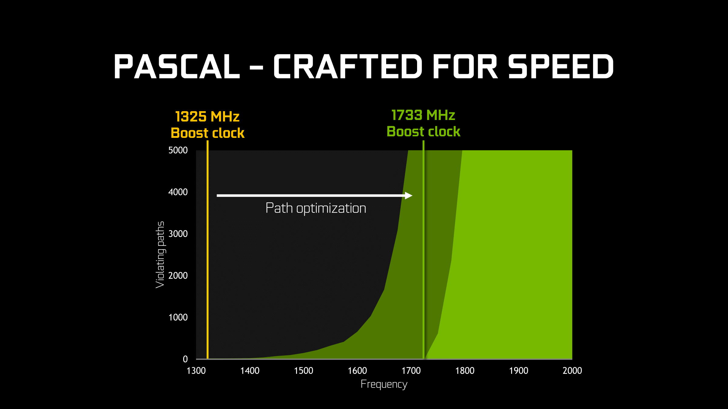
From an implementation point of view this isn’t the first time that NVIDIA has pushed for high clockspeeds, as most recently the 40nm Fermi architecture incorporated a double-pumped shader clock. However this is the first time NVIDIA has attempted something similar since they reined in their power consumption with Kepler (and later Maxwell). Having learned their lesson the hard way with Fermi, I’m told a lot more care went into matters with Pascal in order to avoid the power penalties NVIDIA paid with Fermi, exemplified by things such as only adding flip-flops where truly necessary.
Meanwhile when it comes to the architectural impact of designing for high clockspeeds, the results seem minimal. While NVIDIA does not divulge full information on the pipeline of a CUDA core, all of the testing I’ve run indicates that the latency (in clock cycles) of the CUDA cores is identical to Maxwell. Which goes hand in hand with earlier observations about throughput. So although optimizations were made to the architecture to improve clockspeeds, it doesn’t look like NVIDIA has made any more extreme optimizations (e.g. pipeline lengthening) that detectably reduces Pascal’s per-clock performance.
Finally, more broadly speaking, while this is essentially a one-time trick for NVIDIA, it’s an interesting route for them to go. By cranking up their clockspeeds in this fashion, they avoid any real scale-out issues, at least for the time being. Although graphics are the traditional embarrassingly parallel problem, even a graphical workload is subject to some degree of diminishing returns as GPUs scale farther out. A larger number of SMs is more difficult to fill, not every aspect of the rendering process is massively parallel (shadow maps being a good example), and ever-increasing pixel shader lengths compound the problem. Admittedly NVIDIA’s not seeing significant scale-out issues quite yet, but this is why GTX 980 isn’t quite twice as fast as GTX 960, for example.
Just increasing the clockspeed, comparatively speaking, means that the entire GPU gets proportionally faster without shifting the resource balance; the CUDA cores are 43% faster, the geometry frontends are 43% faster, the ROPs are 43% faster, etc. The only real limitation in this regard isn’t the GPU itself, but whether you can adequately feed it. And this is where GDDR5X comes into play.


200 Comments
View All Comments
Ryan Smith - Friday, July 22, 2016 - link
2) I suspect the v-sync comparison is a 3 deep buffer at a very high framerate.lagittaja - Sunday, July 24, 2016 - link
1) It is a big part of it. Remember how bad 20nm was?The leakage was really high so Nvidia/AMD decided to skip it. FinFET's helped reduce the leakage for the "14/16"nm node.
That's apples to oranges. CPU's are already 3-4Ghz out of the box.
RX480 isn't showing it because the 14nm LPP node is a lemon for GPU's.
You know what's the optimal frequency for Polaris 10? 1Ghz. After that the required voltage shoots up.
You know, LPP where the LP stands for Low Power. Great for SoC's but GPU's? Not so much.
"But the SoC's clock higher than 2Ghz blabla". Yeah, well a) that's the CPU and b) it's freaking tiny.
How are we getting 2Ghz+ frequencies with Pascal which so closely resembles Maxwell?
Because of the smaller manufacturing node. How's that possible? It's because of FinFET's which reduced the leakage of the 20nm node.
Why couldn't we have higher clockspeeds without FinFET's at 28nm? Because power.
28nm GPU's capped around the 1.2-1.4Ghz mark.
20nm was no go, too high leakage current.
16nm gives you FinFET's which reduced the leakage current dramatically.
What does that enable you to do? Increase the clockspeed..
Here's a good article
http://www.anandtech.com/show/8223/an-introduction...
lagittaja - Sunday, July 24, 2016 - link
As an addition to the RX 480 / Polaris 10 clockspeedGCN2-GCN4 VDD vs Fmax at avg ASIC
http://i.imgur.com/Hdgkv0F.png
timchen - Thursday, July 21, 2016 - link
Another question is about boost 3.0: given that we see 150-200 Mhz gpu offset very common across boards, wouldn't it be beneficial to undervolt (i.e. disallow the highest voltage bins corresponding to this extra 150-200 Mhz) and offset at the same time to maintain performance at lower power consumption? Why did Nvidia not do this in the first place? (This is coming from reading Tom's saying that 1060 can be a 60w card having 80% of its performance...)AnnonymousCoward - Thursday, July 21, 2016 - link
NVIDIA, get with the program and support VESA Adaptive-Sync already!!! When your $700 card can't support the VESA standard that's in my monitor, and as a result I have to live with more lag and lower framerate, something is seriously wrong. And why wouldn't you want to make your product more flexible?? I'm looking squarely at you, Tom Petersen. Don't get hung up on your G-sync patent and support VESA!AnnonymousCoward - Thursday, July 21, 2016 - link
If the stock cards reach the 83C throttle point, I don't see what benefit an OC gives (won't you just reach that sooner?). It seems like raising the TDP or under-voltaging would boost continuous performance. Your thoughts?modeless - Friday, July 22, 2016 - link
Thanks for the in depth FP16 section! I've been looking forward to the full review. I have to say this is puzzling. Why put it on there at all? Emulation would be faster. But anyway, NVIDIA announced a new Titan X just now! Does this one have FP16 for $1200? Instant buy for me if so.Ryan Smith - Friday, July 22, 2016 - link
Emulation would be faster, but it would not be the same as running it on a real FP16x2 unit. It's the same purpose as FP64 units: for binary compatibility so that developers can write and debug Tesla applications on their GeForce GPU.hoohoo - Friday, July 22, 2016 - link
Excellent article, Ryan, thank you!Especially the info on preemption and async/scheduling.
I expected the preemption mght be expensive in some circumstances, but I didn't quite expect it to push the L2 cache though! Still this is a marked improvement for nVidia.
hoohoo - Friday, July 22, 2016 - link
It seems like the preemption is implemented in the driver though? Are there actual h/w instructions to as it were "swap stack pointer", "push LDT", "swap instruction pointer"?