The NVIDIA GeForce GTX 1080 & GTX 1070 Founders Editions Review: Kicking Off the FinFET Generation
by Ryan Smith on July 20, 2016 8:45 AM ESTGP104’s Architecture
Looking at an architecture diagram for GP104, Pascal ends up looking a lot like Maxwell, and this is not by chance. After making more radical changes to their architecture with Maxwell, for Pascal NVIDIA is taking a bit of a breather. Which is not to say that Pascal is Maxwell on 16nm – this is very much a major feature update – but when it comes to discussing the core SM architecture itself, there is significant common ground with Maxwell.
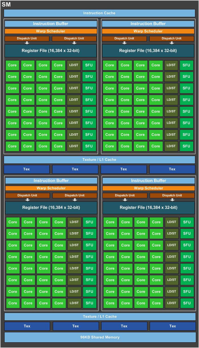
We’ll start with the GP104 SM. Simply named the SM for this generation – NVIDIA has ditched the generational suffix due to the potential for confusion with the used-elsewhere SMP – the GP104 SM is very similar to the Maxwell SM. We’re still looking at a single SM partially sub-divided into four pieces, each containing a single warp scheduler that’s responsible for feeding 32 CUDA cores, 8 load/store units, and 8 Special Function Units, backed by a 64KB register file. There are two dispatch ports per warp schedule, so when an instruction stream allows it, a warp scheduler can extract a limited amount of ILP with an instruction stream by issuing a second instruction to an unused resource.
Meanwhile shared between every pair of sub-partitions is 4 texture units and the combined L1/texture cache, again unchanged from Maxwell. Finally, we have the resources shared throughout the whole SM: the 96KB shared memory, the instruction cache, and not pictured on NVIDIA’s diagrams, the 4 FP64 CUDA cores and 1 FP16x2 CUDA core.
Overall then at the diagram level the GP104 SM looks almost identical to the Maxwell SM, but with one exception: the PolyMorph Engine. Although the distinction is largely arbitrary for GP104, the PolyMorph Engine has been moved up a level; it’s no longer part of the SM, but rather part of the newly re-introduced TPC, which itself sits between the GPC and the SM.
The TPC exists because although GP104 still has a 1:1 ratio between PolyMorph Engines and SMs, the Pascal architecture itself allows for different SM configurations, which is in turn used on GP100 to allow it to have multiple smaller SMs of 64 CUDA Cores. For GP100 the TPC allows for multiple SMs to share a PolyMorph Engine, but for GP104 there’s no sharing involved. To that end the TPC as an organizational unit technically exists across all Pascal parts, but it has no real significance for GP104. In fact it doesn’t even have a real name; NVIDIA reused the acronym from earlier DX10 architectures, where the TPC was the name assigned to the Texture Processor Cluster.
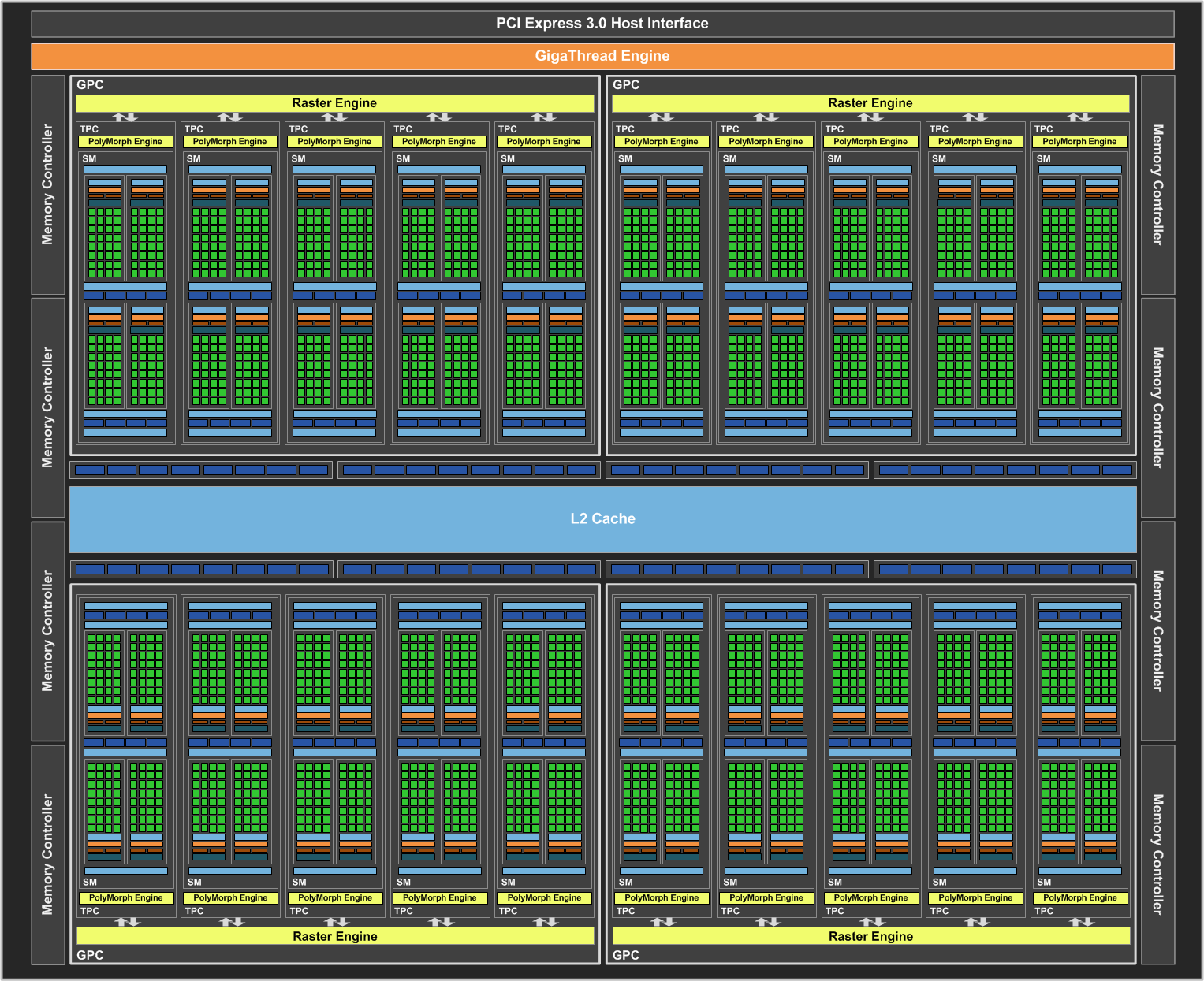
Looking at the bigger picture of the complete GP104 GPU, the similarities continue between GP104 and GM204. GP104’s SMs are clustered five-a-piece inside of the GPC, with each cluster sharing a single Raster Engine. Overall there are 4 such GPCs, giving us 20 SMs altogether. Compared to GM204 then, we’re looking at the same number of GPCs, with each GPC having gained 1 SM.
Things get more interesting when we look at the back end of the rendering/execution pipeline, which is comprised of the L2 cache, ROPs, and memory controllers. The ROP/L2 count has not changed relative to GM204 – we still have 64 ROPs paired up with a total of 2MB of L2 cache – however the memory controller count has. And with it the logical configuration of the ROP/L2 blocks have changed as well.
Whereas GM204 had 4 64bit GDDR5 memory controllers, each connected to 2 or 4 memory chips, GP104 breaks that down further to 8 32bit GDDR5X memory controllers, each of which is connected to 1 memory chip on GTX 1080. I’ll go into greater detail on GDDR5X a bit later, but the significance of this backend organizational change has to do with the introduction of GDDR5X. Because GDDR5X reads and writes data in 64B amounts (versus 32B amounts on GDDR5), NVIDIA has reorganized the memory controllers to ensure that each memory controller still operates on the same amount of data. With GDDR5 they teamed up two GDDR5 channels to get 64B operations, whereas with GDDR5X this can be accomplished with a single memory channel.
This in turn is where the ROP reorganization comes from. As there’s a 1:1 relationship between ROP partitions and memory controllers, the 64 ROPs are now broken up into 8 partitions for GP104, as opposed to 4 partitions on GM204. There are some performance tradeoffs that come from having more ROP partitions, but to the best of my knowledge these should not be significant.
Meanwhile the new GDDR5X memory controllers are also backwards compatible with traditional GDDR5, which in turn is used to drive the GTX 1070 with its 8Gbps GDDR5. The difference in operation between GDDR5 and GDDR5X does make the ROP situation a bit trickier overall for NVIDIA’s architects – now they need to be able to handle two different memory access patterns – though for NVIDIA this isn’t a wholly new problem. Previous generation architectures have supported both GDDR5 and DDR3, the two of which have their own differences in memory access patterns.
In a by-the-numbers comparison then, Pascal does not bring any notable changes in throughput relative to Maxwell. CUDA cores, texture units, PolyMorph Engines, Raster Engines, and ROPs all have identical theoretical throughput-per-clock as compared to Maxwell. So on a clock-for-clock, unit-for-unit basis, Pascal is not any faster on paper. And while NVIDIA does not disclose the size/speed of most of their internal datapaths, so far I haven’t seen anything to suggest that these have radically changed. This continuity means that outside of its new features, GP104 behaves a lot like GM204. Though it should be noted that real world efficiency isn’t quite as cut and dry, as various factors such as the increased SM count and changes in memory technology can greatly influence this.


200 Comments
View All Comments
jcardel - Wednesday, July 27, 2016 - link
This is excactly the same situation as me. I got a 770 sitting in my rig, and am looking hard at the 1070, maybe soon. Although my 770 is still up to the task in most games, I really play only blizzard games theese days and they are not hard on your hardware.My biggest issue is really that it is rather noisy, so I will be looking for a solution with the lowest DB.
Great article, it was totally worth waiting for.. I only read this sort of stuff here so have been waiting till now for any 1080 review.
Thanks!
D. Lister - Thursday, July 21, 2016 - link
Nice job, Ryan. Good comeback. Keep it up.Saeid92 - Thursday, July 21, 2016 - link
What is 99th procentile framerate?Ryan Smith - Thursday, July 21, 2016 - link
If you sorted the framerate from highest to lowest, this would be the framerate of the slowest 1%. It's basically a more accurate/meaningful metric for minimum frame rates.Eris_Floralia - Thursday, July 21, 2016 - link
This is why I love Anandtech. Deep in reviews. Well I even wanted to be one of your editors if you have the plan to create a Chinese transtate version of these reviews.daku123 - Thursday, July 21, 2016 - link
Typo on FP16 Throughput page. In second paragraph, it should be Tegra X1 (not Tesla X1?).Ryan Smith - Thursday, July 21, 2016 - link
Eyup. Thanks!Badelhas - Thursday, July 21, 2016 - link
Great detailed review, as always. But I have to ask once again:why didnt you do some kind of VR Benchmarks? Thats what drives my choises now, to be honest.
Cheers
Ranger1065 - Thursday, July 21, 2016 - link
After over 2 months of reading GTX1080 reviews I felt a distinct lack of excitementas I read Anandtech kicking off their review of the finfet generation. Could it
prove to be anything but an anticlimax?
Sadly and unsurprisingly...NOT.
It was however amusing to see the faithfull positively gushing praises for Anandtech
now that the "greatly anticipated" review is finally out.
Yes folks, 20 or so pages of (well written) information, mostly already covered by other tech sites,
finally published, it's as if a magic wand has been waved, the information has been presented with
that special Anandtech sauce, new insights have been illuminated and all is well in Anandtechland again.
(AT LEAST UNTIL THE NEXT 2 MONTH DELAY.) LOL.
I do like the way Anandtech presents the FPS charts.
Back to sleep now Anandtech :)
mkaibear - Thursday, July 21, 2016 - link
You've hit the nail on the head here Ranger.The info which is included within the article is indeed mostly already covered by other tech sites.
Emphasis on the "mostly" and the plural "sites".
Those of us who have jobs which keep us busy and have an interest in this sort of thing often don't have the time to trawl round many different sites to get reviews and pertinent technical data so we rely upon those sites which we trust to produce in-depth articles, even if they take a bit longer.
As an IT Manager for (most recently) a manufacturing firm and then a school, I don't care about bleeding edge, get the new stuff as soon as it comes out, I care about getting the right stuff, and a two month delay to get a proper review is absolutely fine. If I need quick benchmarks I'll use someone like Hexus or HardOCP but to get a deep dive into the architecture so I can justify purchases to the Art and Media departments, or the programers is essential. You don't get that anywhere else.