Examining Soft Machines' Architecture: An Element of VISC to Improving IPC
by Ian Cutress on February 12, 2016 8:00 AM EST- Posted in
- CPUs
- Arm
- x86
- Architecture
- Soft Machines
- IPC
Soft Machines
To put it succinctly, having a thread take resources from multiple cores - when the performance can be extracted - sounds like the long-desired solution to the problem making multi-core designs more useful in lightly-threaded scenarios. Having multiple threads use resources on a single core on the same clock cycle is an even bigger leap in the same direction. Now obviously Soft Machines didn’t come up with this overnight.
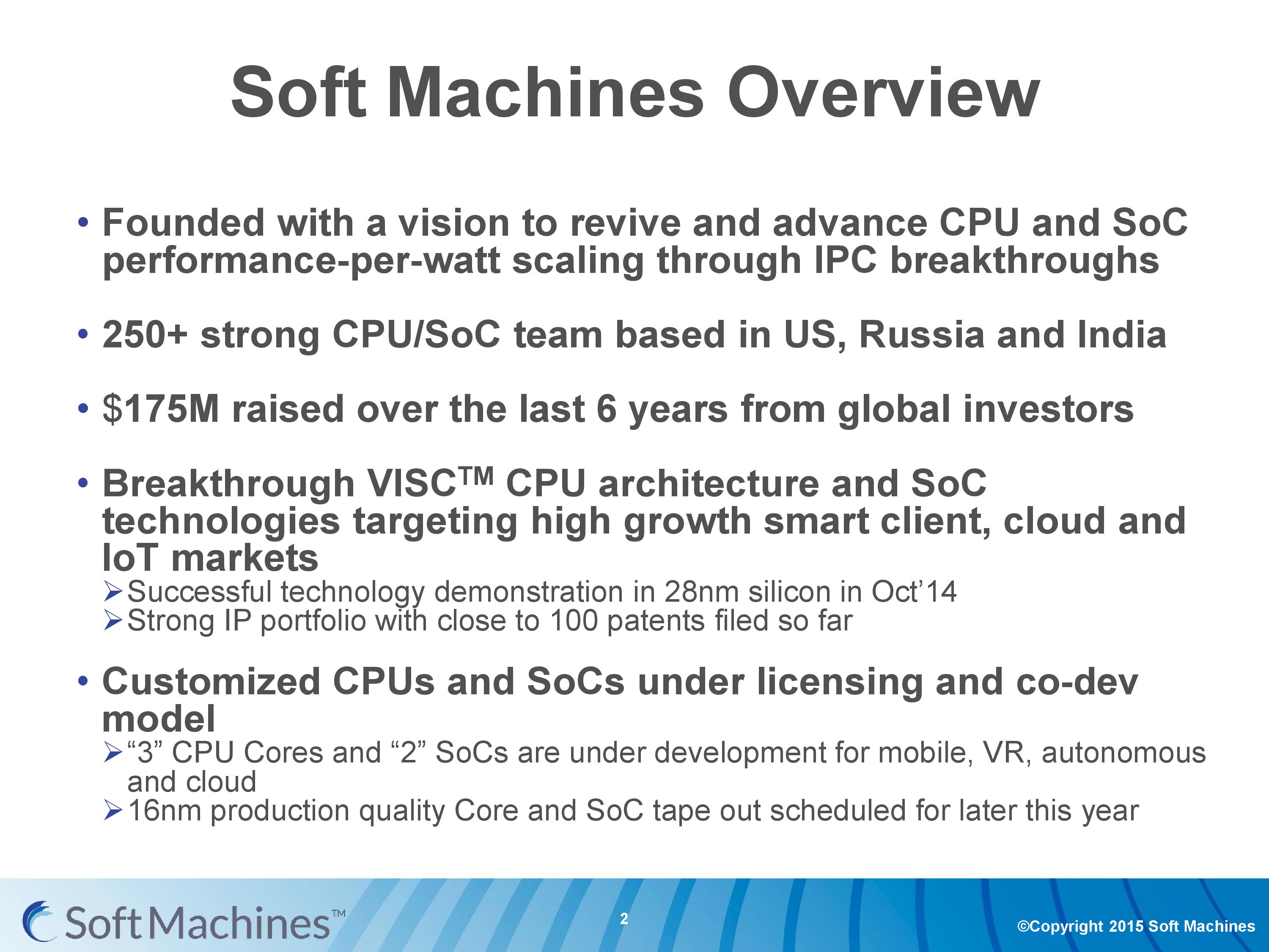
Soft Machines came out of stealth mode at the 2014 Linley Conference. Their main goal was to increase performance-per-watt using better IPC designs, which is often one of the better ways if you can keep a design fed with data. One big challenge to this is that IPC has been somewhat flat these past few years - we're seeing small sub-10% yearly increases from the big players using standard designs. Soft Machines were already six years old at the time, with $150M+ raised from investors that include Samsung Ventures, GlobalFoundries, AMD, Mubadala and others (with another $25M since). If those names all seem interlinked, it’s because they all have historic business or investment dealings with each other (AMD/GloFo, Samsung/GloFo, AMD/Mubadala etc.). The team at Soft Machines is 250+ strong, with ex Intel, ex Qualcomm, ex AMD engineers on staff from processor design to platform architects. Half the staff is currently located in California.
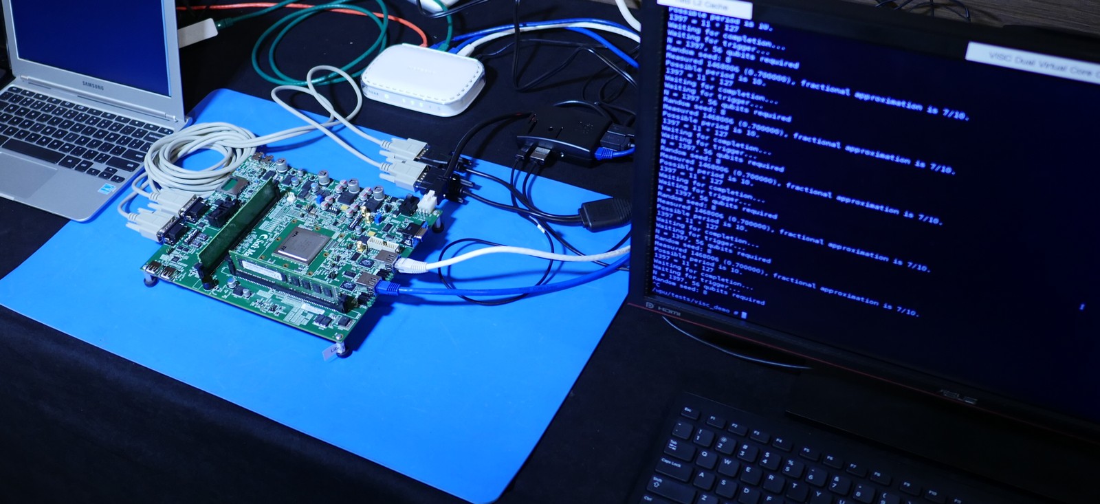
At the 2014 conference, aside from explaining what they were doing, Soft Machines also exhibited working silicon of their design. The first generation proof of concept was fabbed at 28nm at TSMC and running at 500 MHz.
It seems odd to say that it was done at TSMC, especially with Samsung and Global Foundries as investors. We were told that this was due to timing and positioning with IP more than anything else, and the same is true for the next generation at 16nm FF+, rather than 14nm.
VISC and Roadmaps
The first generation chip wasn’t perfect – there were some design flaws in silicon that required specific workarounds relating to cache flushing and various methods, but at the time it was compared to a single thread Cortex A15 running at a similar frequency in a Samsung processor. The results with SPEC2000, SPEC2006, Denbench and Kraken gave a corresponding IPC relative to A15 of 1.5x to 7x, or as Soft Machines likes to put it: 3-4x "on average." It was estimated that access to a second physical core improves performance by an average of 50-60%, or an average IPC of 1.3 per core compared to 0.71 for Cortex A15, which explains the 3-4x average.
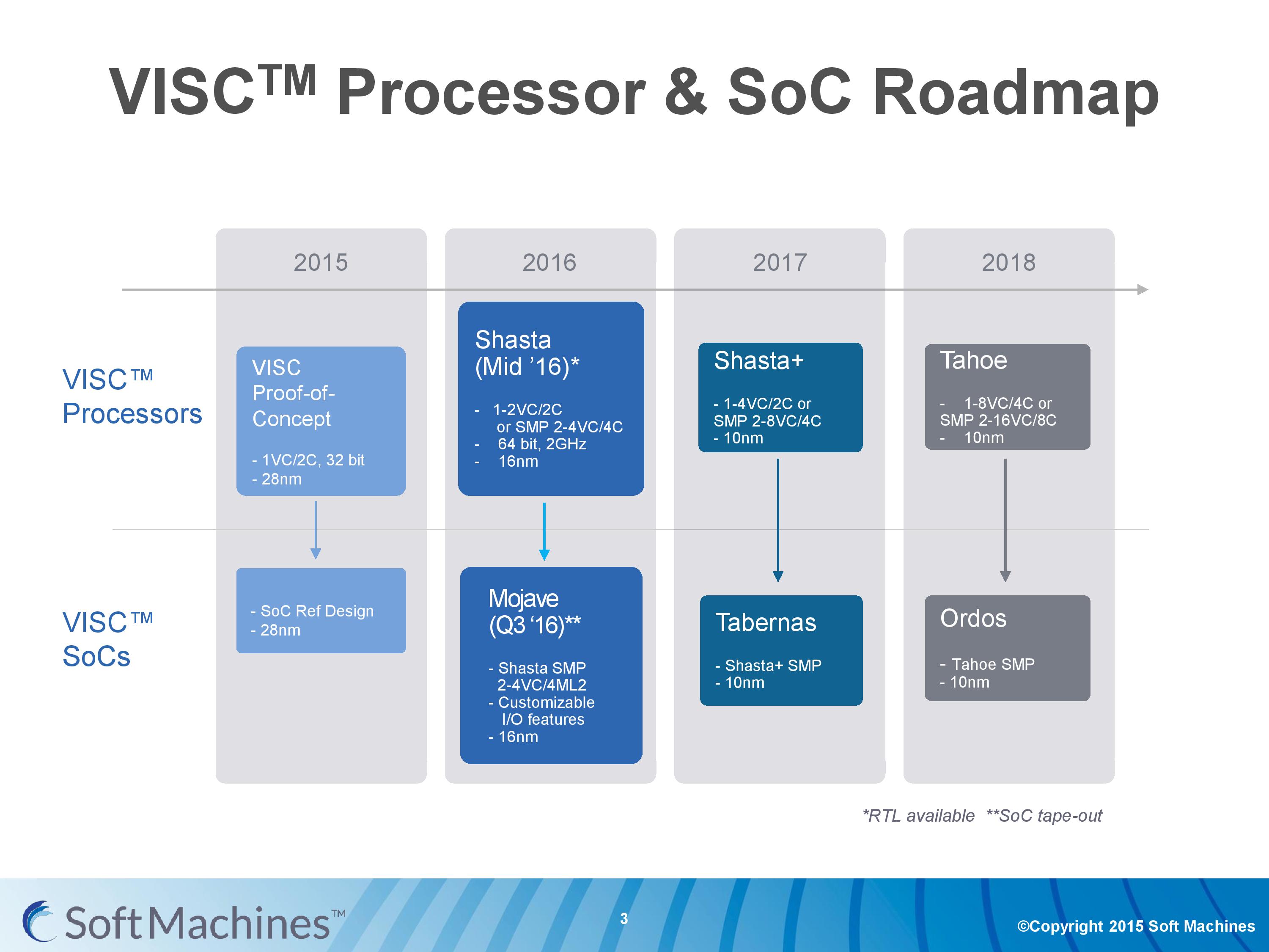
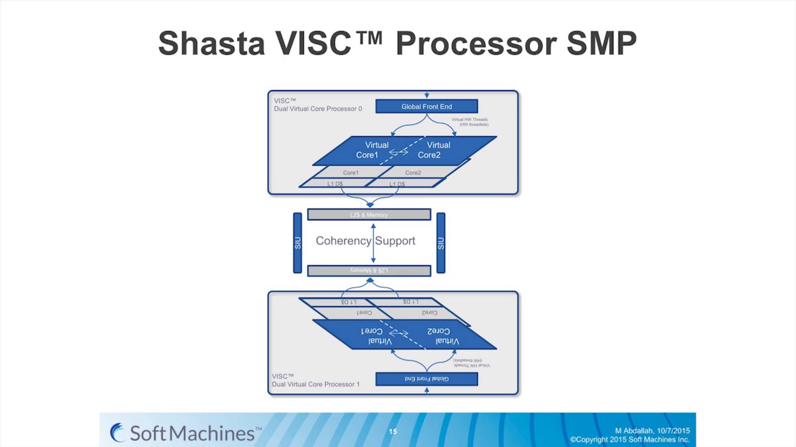
The roadmap for Soft Machines put their second generation VISC core, Shasta, in line for 2016. It was formally announced at the 2015 Linley Conference, with this month’s announcement being more about availability for licensing on 16FF+. The Shasta core on this node is designed as a 2C/2VC design, or two of these can be put together using a custom protocol interconnect to form a dual 2C/2VC design.
The custom interconnect fabric here is capable of over 200 GB/s, although in current designs only a single interface is present, allowing only two chips to be connected.
The dual processor design is going to be part of the Mojave IP as a fully integrated SoC.
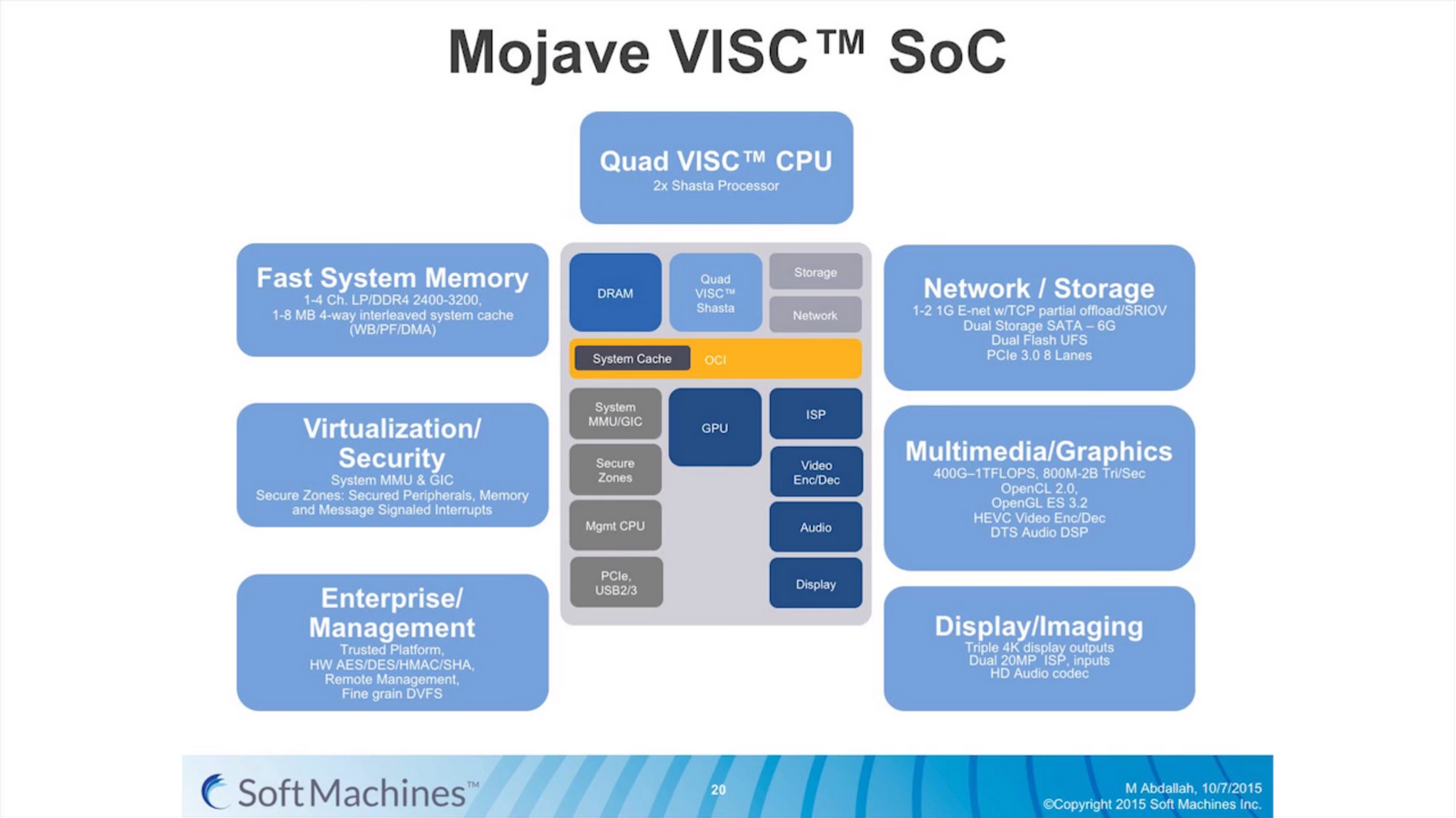
Along with the requisite VISC cores, the Mojave SoC includes PowerVR graphics, a DDR4 memory controller, virtualization management, a PCIe root complex capable of eight lanes of PCIe 3.0, USB ports, support for SATA, UFS, OpenCL 2.0 and other standards.
Looking forward, Soft Machines would like to see production move to 10nm in 2017 to take advantage of further power and area scaling. Meanwhile along that same timeframe they also want to expand the Shasta design to allow for four virtual cores per two physical cores, essentially allowing more threads to be in flight at one time and fully use the resources better. 2018 sees the move to four physical cores and eight virtual cores per design, while still supporting SMP and SoC designs as well.


97 Comments
View All Comments
KAlmquist - Sunday, February 14, 2016 - link
If I understand the article correctly, the difference between VISC and SMT is that in SMT there is a single scheduler which manages all of the execution units. VISC implements a two stage scheduling algorithm. In the first stage, an operation is assigned to a core. In the second stage, the scheduler for that core assigns the operation to an execution unit.The downside of SMT is that the amount of silicon required to implement the scheduler grows faster than the number of execution units. So as you add more threads and more execution units, it becomes harder and harder to keep the cost of the scheduler to a reasonable level.
In the second stage of VISC, you have multiple schedulers, each feeding a small number of execution units, which keeps these schedulers simple. In the first stage, the schedulers require at least some awareness of all the execution units. For example, if you have an integer multiply instruction, you want to send it to a core that doesn't have other integer multiply operations outstanding rather than just chosing the core with the smallest total number of outstanding operations. What may keep the first stage scheduling reasonably simple is that it doesn't appear to do any instruction reordering (though it does have to do the bookwork to keep track of which instructions have been retired).
In short, VISC appears to be intended to scale better than SMT as you add more threads and execution units.
What is strange, then, is that Soft Machines isn't talking about building an 8 thread device like IBM's POWER8. Instead, they have a two and four thread designs, and are mostly talking about the former. A two thread VISC design makes sense only if you believe that the SMT approach is already hitting its limits with two threads.
My sense is that VISC is not going to be a game changer, but Soft Machines could be successful if ARM Holdings screws up. If ARM has has a major screw up technologically (like AMD did with Bulldozer), Soft Machines could end up with a superior product. Conversely, if ARM screws up on customer relations, all Soft Machines would need is something close to technological parity with ARM to win customers.
Shadowmaster625 - Monday, February 15, 2016 - link
When Intel purchased Altera I immediately began to visualize all sorts of great potential breakthroughs in single threaded IPC. I imagine that within 5 years, we will have at least a modest number of FPGA cells integrated within Intel CPU cores. These cells will be programmed on-the-fly with application specific DSPs that will be capable of completing commonly used combinations of instructions MUCH faster than the general x86 instruction set would allow. I expect this to be the singularly largest breakthrough in computing of the last 20 years. Within 10 years, I expect the CPU itself to create its own DSP code on the fly as it profiles its own instruction loading in real time. The potential here is utterly massive. Think about what ASICs have done for bitcoin mining... Soon they will be able to do that for javascript!FunBunny2 - Monday, February 15, 2016 - link
-- capable of completing commonly used combinations of instructions MUCH faster than the general x86 instruction set would allow. I expect this to be the singularly largest breakthrough in computing of the last 20 years.that's what the real cpu/RISC core/micro-architecture has done for decades. twerked continually.
-- I imagine that within 5 years, we will have at least a modest number of FPGA cells integrated within Intel CPU cores.
done: http://www.extremetech.com/extreme/184828-intel-un...
"This new Xeon+FPGA chip will fit in the standard E5 LGA2011 socket, but the integrated FPGA will allow each chip to be customized to specific workloads."
Shadowmaster625 - Monday, February 15, 2016 - link
That's not what I mean. That is of course a good start, but what I'm talking about is programmable logic linked tightly to the actual execution units of the CPU core. Smaller blocks, probably only a square millimeter or perhaps even less. But many of them. Just like Skylake has 6 execution units. One of these programmable blocks would be only about the same size as one of those existing execution units. They would have direct access to the prefetcher and scheduler and instruction/data caches. They would be power gated.dustwalker13 - Saturday, February 20, 2016 - link
yes it looks good on paper ... but up to now that is all that it does.silicon existing at HQ is so much smoke and mirrors until some independant source has an actual go at it and publishes results.
it looks promising, but so did a million other things that ended up as just another failiur or worse scam.
i will keep an eye on this one but for now there simply is nothing to see than mirror images produced by a lot of hot air.
mikato - Saturday, February 20, 2016 - link
So why did they come out of stealth mode?TruePath - Saturday, April 16, 2016 - link
I've been curious for a long time why more wasn't done to use parallel resouces to extract instruction level parrelism.However, what puzzles me is why do so much of the work on the fly at run time. Sure, one needs to be able to respond to dynamic performance information like failed speculation but it seems like there is substantial overhead in translating the host ISA into native instructions and (I assume) encoding information into the native instructions about resource needs and dependencies.
Even before a program is run knowledge of the exact processor would enable software to translate the ISA (targeting the exact chip), hint at resources needs and perform a degree of instruction reordering (over a larger window than in hardware).
So why not push as much of this into the software as possible. One can even cache the results of software ISA translation. Is it just a desire to be totally hardware compatible?