VIA Introduces Quad Band Memory - 2X DDR at 1X Prices
by Anand Lal Shimpi on September 17, 2002 1:49 PM EST- Posted in
- CPUs
QBM: How it works
A QBM module starts off just like a regular DDR SDRAM module but with a minimum of 16 DDR SDRAM devices on the module itself. Eight of these devices belong to the first bank, and the other eight belong to the second bank - one on each side of the DIMM. What we've just described is identical to a double sided DDR SDRAM DIMM with 16 chips. As we've mentioned before, a QBM module still has the same 184-pin interface as a conventional DDR DIMM.
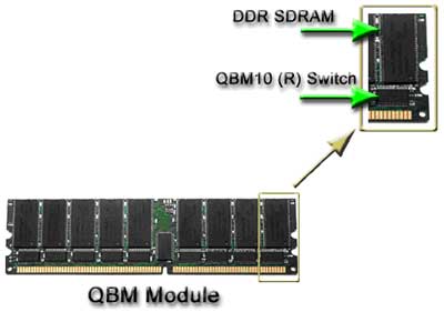
Here's where the difference between QBM and conventional modules comes into play; QBM modules will have a set of 8 registers (QBM-10) as well as a phase-locked loop (PLL). The purpose of the PLL is to take the incoming clock signal from the chipset and shift it by 90 degrees; this shifted signal is then fed to the second bank of the DIMM, while the first bank receives the unaltered clock directly from the chipset.
The 8 registers then switch between which bank gets to transfer data every clock; because of the 90 degree phase shift, there is a slight delay in transferring data from the second bank but both transfers actually end up happening within a single clock cycle. The end result is that you get two DDR transfers per clock, or 4 bits of data are sampled per clock thus doubling the throughput of DDR (hence the name Quad Band Memory).
|
Memory
Bandwidth Comparison
|
|||
| Memory Type |
Bandwidth
|
||
| DDR266 |
2.1GB/s
|
||
| DDR333 |
2.7GB/s
|
||
| Dual Channel DDR266 |
4.2GB/s
|
||
| Dual Channel DDR333 |
5.3GB/s
|
||
| QBM533 |
4.2GB/s
|
||
| QBM667 |
5.3GB/s
|
||


0 Comments
View All Comments