The Future of CPU Packaging: Intel's BBUL
by Anand Lal Shimpi on October 8, 2001 8:30 PM EST- Posted in
- CPUs
Bumpless Build-Up Layer: The Future of Packaging
While AMD has taken the performance crown from Intel on numerous occasions, AMD cannot compete with Intel's manufacturing capabilities. Intel actually has a branch whose sole purpose is to deal with packaging and the needs of tomorrow's processors. Intel has been talking about 1 billion transistors in a chip running at 10GHz+, so it's no surprise that they have 900 people working on packaging technologies.
Intel's Assembly Technology Development team is 900 people strong with most of them located in Arizona. And it is out of Arizona that today's announcement on a breakthrough in packaging technology is made.
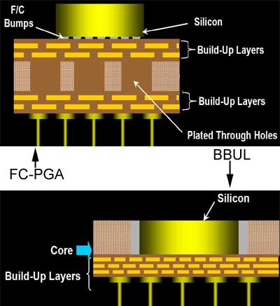
Although the technology won't be put to use for another 5 or 6 years, Intel's Bumpless Build-Up Layer (BBUL) will definitely change the face of packaging. The beauty of BBUL is that the silicon is actually integrated into the die. A BBUL CPU will be manufactured by building the package one layer at a time and embedding the silicon into the package after testing. Remember the issue of the flip-chip solder bump density? That is no longer an issue with BBUL since there are no more solder bumps; the silicon is directly embedded in the package. Another benefit of this is that since the core is no longer raised, there is no potential for any chipped/cracked cores due to improperly installed heatsinks. Intel did mention however that they would probably still use heatspreaders with this technology meaning that you wouldn't be able to chip/crack the cores in any case.
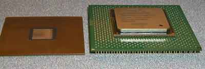
This also brings the silicon closer to the capacitors on the bottom of the CPU, increasing power delivery efficiency as we mentioned earlier. The package is also physically thinner, and as you can see from the following pictures it is a lot thinner (note: the prototype BBUL chip used a core approximately the size of Intel's 0.13-micron Northwood core and didn't have any pins attached to it. The final chips will obviously have pins. All photos were courtesy of Intel Corporation).
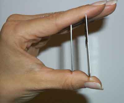
Left: BBUL Prototype Chip, Right: A Credit Card
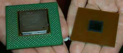
Left: Pentium 4 Chip, Right: BBUL Prototype Chip
The benefits of this type of packaging can also be extended to multi-core CPUs. One of the major problems with outfitting a CPU with two cores is that the two must be tested together in the final CPU and if just one is bad, the entire CPU must be thrown away (AMD's SledgeHammer will unfortunately face this problem it seems). With BBUL you'll be able to embed two CPU cores using two separate dies and connect them with an internal high-speed bus, giving you the benefits of a multi-core CPU but also allowing you to test the cores individually before packaging them into a single CPU.
Final Words
We don't normally get the chance to present articles like this to you, but we hope you enjoyed the content. Intel's BBUL is definitely a step forward in CPU packaging technologies and it will be useful to all manufacturers since the technology can be used to package chipsets, integrate higher performance graphics cores in North bridges, and even offer very high performance L3 cache integrated into a multi-chip processor module.


4 Comments
View All Comments
Googer - Sunday, January 16, 2005 - link
I cannot beleive after 4 years no one has chosen to comment on such important technology such as this. As of right now Intel has chosen to delay the future of this technology.VasileRT - Thursday, August 19, 2010 - link
It seems that Intel is finally geting started on this. They are currently hiring for this project.extide - Monday, September 10, 2012 - link
It is kinda interesting to read this article 11 years later, and see how things have changed. See what stuff came true and what didn't :)Piyush patel - Thursday, March 21, 2019 - link
Nice post also know about the cpu packaging <a href="https://www.cyberlearningservices.com/2019/03/cpu-... Click Here <\a>.