SiS 730S Socket-A Chipset: Is the Duron allowed to succeed now?
by Anand Lal Shimpi on December 13, 2000 4:06 AM EST- Posted in
- CPUs
A chip called Homer
Going by the codename ‘Homer’ (not from the Simpsons but Homer as in the storyteller that brought us The Iliad and The Odyssey), the 730S is a very unique solution. We are used to chipsets having two major components, a Northbridge and a Southbridge, or in the case of Intel 8xx chipsets, a Memory Controller Hub (MCH) and a I/O Controller Hub (ICH).
The Northbridge or MCH houses the memory and graphics controllers and provides the interface to the CPU as well. This leaves the Southbridge or ICH to handle the USB ports, IDE channels and PCI devices, among other tasks.
The two are usually connected via the PCI bus running at 33MHz (133MB/s) or in the case of Intel’s Hub Architecture, the two chips are connected via a Hub Interface running at 133MHz (double pumped = 266MB/s bandwidth).
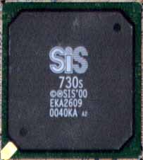
The 730S deviates from this tradition, as it is a single chip solution. This isn’t to say that the 730S doesn’t have a Northbridge and a Southbridge connected by a PCI bus, all it means is that the North and Southbridges are contained within a single chip. This chip is the 672-pin 730S.
This obviously saves space on the motherboard since manufacturers only have to make room for a single chip in their design and thus drives the cost of the overall solution down right from the start. Also, by moving to a single chip design, the traces that would otherwise be routed from the Southbridge up to the Northbridge are no longer necessary since all connections are now contained internally within the 730S chip itself.
To bring the integrated nature of the 730S chipset up to the next level, the single chip also features an on-die graphics controller, which is exactly what the Duron needs in order to be successful in the cutthroat value PC market. The 730S makes use of the SiS 300 graphics core, which, being a solution made by SiS themselves, is perfectly suited for use with the 730S. As we discovered in our testing, the 730S’ drivers exhibited no problems and the integrated graphics worked flawlessly. Performance-wise, you shouldn’t expect too much from the SiS 300 graphics core; basically it is equivalent to the i810’s integrated graphics.
The one major selling point that the SiS 300 does hold over the competition is that it offers hardware motion compensation and iDCT support. This helps reduce CPU usage while playing DVD/MPEG2 streams, which won’t be too big of a problem with even the slowest Duron processors, but it will help keep those CPU cycles free for whatever other tasks you may throw at your “value PC.” For more information on what this support gives the SiS 300, read our article on DVD Quality, Features and Performance.
The SiS 300 features no integrated frame buffer making it a unified memory architecture (UMA) solution. This means that it shares your system memory using the 64-bit 100/133MHz memory bus. This gives the SiS 300 a very limited amount of memory bandwidth compared to today’s graphics accelerators. More specifically, depending on whether PC100 or PC133 SDRAM is used, the SiS 300 will have a maximum of either 800MB/s or 1.06GB/s of available memory bandwidth. Compared to the “low” 2.7GB/s that the GeForce 256 using SDR memory has, the SiS 300 core obviously won’t be pushing any high frame rates in games. The 300 will pretty much be limited to 640 x 480 x 16 as a playable resolution regardless of the game.


0 Comments
View All Comments