AMD Reveals Polaris GPU Architecture: 4th Gen GCN to Arrive In Mid-2016
by Ryan Smith on January 4, 2016 9:00 AM ESTPolaris: Made For FinFET
The final aspect of RTG’s Polaris hardware presentation (and the bulk of their slide deck) is focused on the current generation FinFET manufacturing processes and what that means for Polaris.
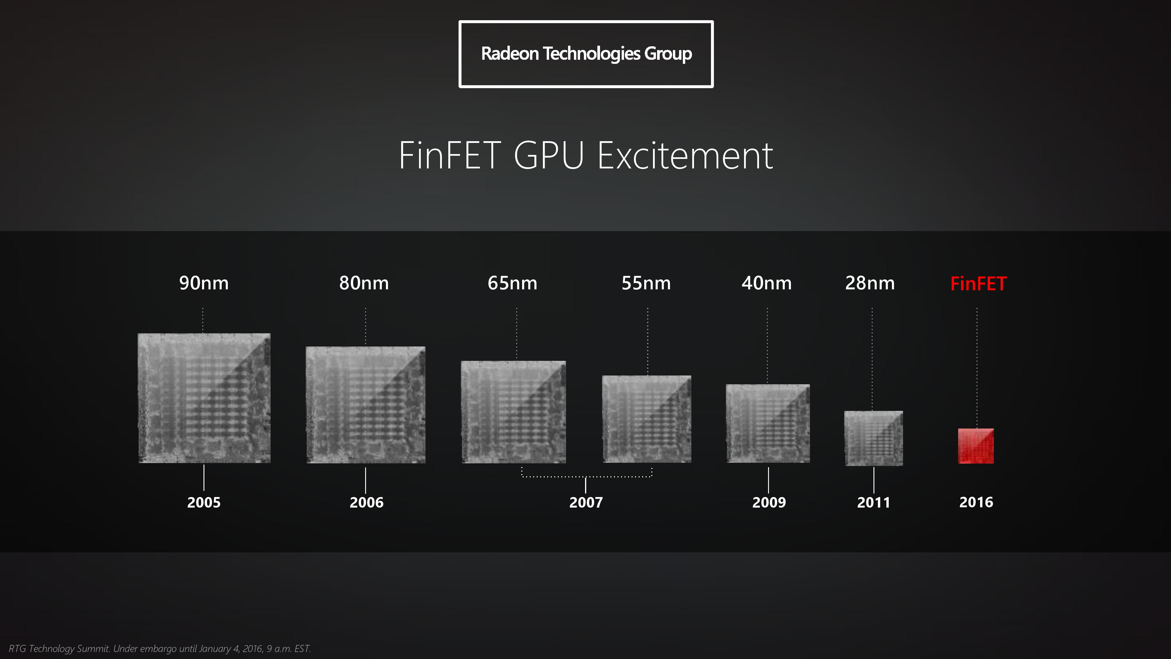
As RTG’s slide concisely and correctly notes, the regular march of progress in semiconductor fabrication has quickly tapered off over the last decade. What was once a yearly cadence of new manufacturing processes – a major new node every 2 years with a smaller step in the intermediate years – became just every two years. And even then, after the 20nm planar process proved unsuitable for GPUs due to leakage, we are now to our fifth year of 28nm planar as the leading manufacturing node for GPUs. The failure of 20nm has essentially stalled GPU manufacturing improvements, and in RTG’s case resulted in GPUs being canceled and features delayed to accommodate the unexpected stall at 28nm.
For their most recent generation of products both RTG and NVIDIA took steps to improve their architectural efficiency due to the lack of a new manufacturing process – with NVIDIA having more success at this than RTG – but ultimately both parties were held back from what they originally were planning back around 2010. So to say that the forthcoming move to FinFET for new GPUs is a welcome change is an understatement; after nearly half a decade of 28nm GPUs we finally will see the kind of true generational improvements that can only come from a new manufacturing node.
To no surprise then, RTG is aggressively targeting FinFET with Polaris and promoting the benefits thereof. With power efficiency essentially being the limiting factor to GPU performance these days, the greatest gains can only be reached by improving overall power efficiency, and for RTG FinFETs will be a big part of getting there. Polaris will be the first RTG architecture designed for FinFETs, and coupled with the architecture improvements discussed earlier, it should result in the largest overall increase in performance per watt for any Radeon GPU family.

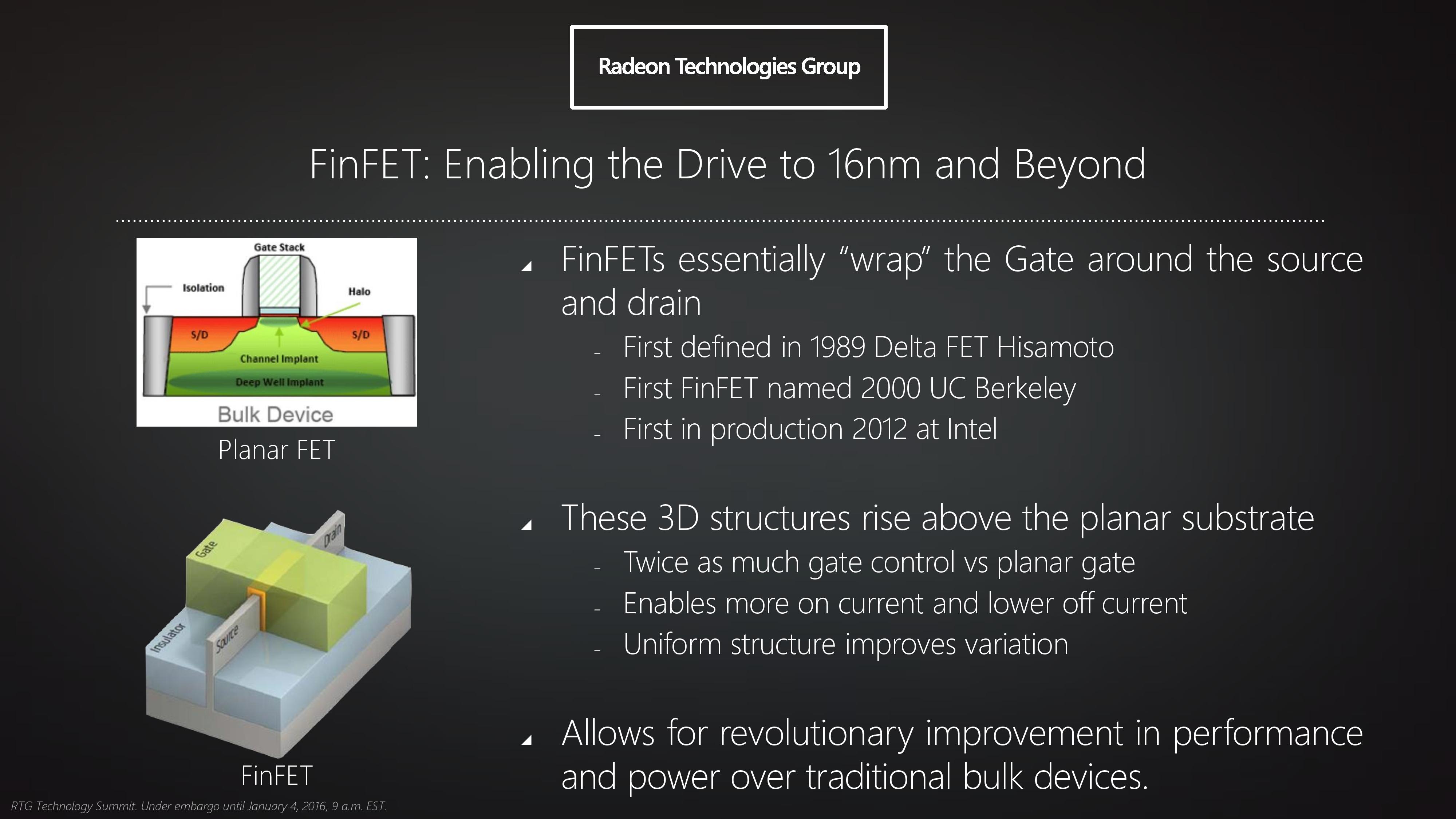
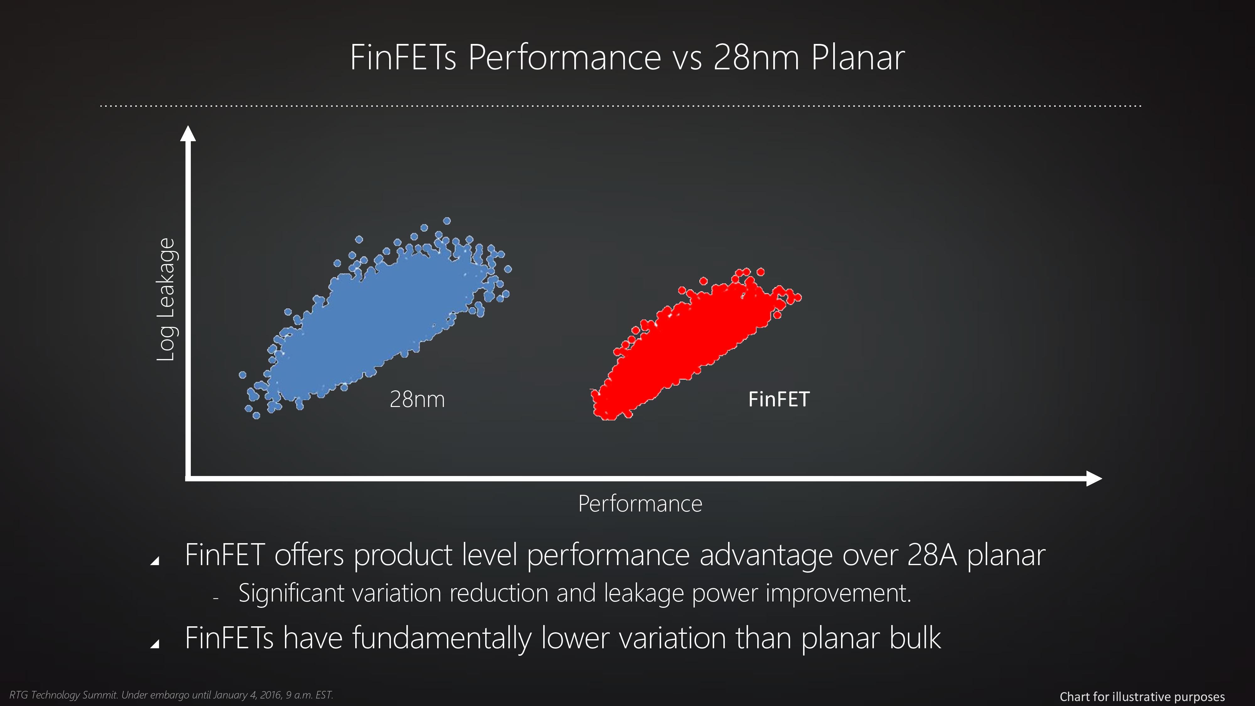
We’ve already covered the technical aspects of FinFET a number of times before, so I’m not going to go into too much depth here. But at the most basic level, FinFETs are the solution to the leakage problems that have made planar transistors impractical below 28nm (and ultimately killed 20nm for GPUs). By using multiple fins to essentially make a transistor 3D, it becomes possible to control leakage in a manner not possible with planar transistors, and that in turn will significantly improve energy efficiency by reducing the amount of energy a GPU wastes just to be turned on.
With the introduction of FinFET manufacturing processes, GPU manufacturing can essentially get back on track after the issues at 20nm. FinFETs will be used for generations to come, and while the initial efficiency gain from adding FinFETs will likely be the single greatest gain, it solves the previous leakage problem and gives foundries a route to 10nm and beyond. At the same time however as far as the Polaris GPUs are concerned, it should be noted that the current generation of 16nm/14nm FinFET processes are not too far removed from 20nm with FinFETs. Which is to say that the move to FinFETs gets GPU manufacturing back on track, but it won’t make up for lost time. 14nm/16nm FinFET is essentially only one generation beyond 28nm by historical performance standards, and the gains we're expecting from the move to FinFET should be framed accordingly.
As for RTG’s FinFET manufacturing plans, the fact that RTG only mentions “FinFET” and not a specific FinFET process (e.g. TSMC 16nm) is intentional. The group has confirmed that they will be utilizing both traditional partner TSMC’s 16nm process and AMD fab spin-off (and Samsung licensee) GlobalFoundries’ 14nm process, making this the first time that AMD’s graphics group has used more than a single fab. To be clear here there’s no expectation that RTG will be dual-sourcing – having both fabs produce the same GPU – but rather the implication is that designs will be split between the two fabs. To that end we know that the small Polaris GPU that RTG previewed will be produced by GlobalFoundries on their 14nm process, meanwhile it remains to be seen how the rest of RTG’s Polaris GPUs will be split between the fabs.
Unfortunately what’s not clear at this time is why RTG is splitting designs like this. Even without dual sourcing any specific GPU, RTG will still incur some extra costs to develop common logic blocks for both fabs. Meanwhile it's also not clear right now whether any single process/fab is better or worse for GPUs, and what die sizes are viable, so until RTG discloses more information about the split order, it's open to speculation what the technical reasons may be. However it should be noted that on the financial side of matters, as AMD continues to execute a wafer share agreement with GlobalFoundries, it’s likely that this split helps AMD to fulfill their wafer obligations by giving GlobalFoundries more of AMD's chip orders.
Closing Thoughts
And with that, we wrap up our initial look at RTG's Polaris architecture and our final article in this series on RTG's 2016 GPU plans. As a high level overview what we've seen so far really only scratches the surface of RTG's plans - and this is very much by design. But as the first occasion of RTG opening up their roadmaps and giving us a bit of a look into the future, it's a welcome change not only for developers, but for the press and public alike.
Backed by the first major node shrink for GPUs in over 4 years, RTG has laid out an aggressive plan for Polaris in 2016. At this point RTG needs to catch up and close the market share gap with NVIDIA - of this RTG is quite aware - and Polaris will be the means to do that. What needs to happen now is for RTG to fully execute on the plans they've laid out, and if they can do so then 2016 should turn out to be an interesting (and competitive) year in the GPU industry.


153 Comments
View All Comments
rrinker - Monday, January 4, 2016 - link
Indeed. Even the GTX 960 tested by HardOCP didn't use 140 watts at full load.Pantsu - Monday, January 4, 2016 - link
The power consumption numbers were from the wall socket.mdriftmeyer - Monday, January 4, 2016 - link
Yes. The Nvidia fans are mentally challenged and don't grasp the baseline system differences between the two are just the card and the Total System Power consumption differences are highlighting the card architectures and FinFET. It seems each one comes in repeats the same mentally challenged thought and leave.DominionSeraph - Monday, January 4, 2016 - link
Using the 950 is like using the 7870XT as an example of Tahiti, or the 5830 for Cypress.Flunk - Monday, January 4, 2016 - link
Yes, would't a Geforce 960m also hit the FPS cap at medium on the X-Wing Map in Battlefront and use a lot less power doing it?Although when it comes to prerelease GPU demos pointless pretty much is par for the course. I'm excited to see how these perform when they're released, as well as Nvidia's Pascal architecture of course.
ToTTenTranz - Monday, January 4, 2016 - link
The GTX 950 uses a cut-down version of GM206, which is nVidia's latest and most power-efficient chip to date.tviceman - Monday, January 4, 2016 - link
GM206 is the least power efficient of all the maxwell chips, by a considerable amount. See the GTX 960 here in the most recent video card review: http://www.techpowerup.com/reviews/Gigabyte/GTX_98...The GTX 950 is even slightly less efficient than the GTX 960: http://www.techpowerup.com/reviews/Gigabyte/GTX_95...
Ch4os - Tuesday, January 5, 2016 - link
22% difference between GM206 and GM204? Oh no, what an mind boggling difference...@Dribble "obviously the AMD chip can only manage 60 hence the cap, but the Nvidia one can manage more."
It isn't obvious, it is one of the possibilities and also the one you chose to roll with.
"there's plenty of nvidia chips that can hit fps and use less power, particularly mobile ones."
And they are also considerably more expensive/rarer since they use hand picked chips and components and still aren't that much more power efficient.
FourEyedGeek - Saturday, January 16, 2016 - link
Still makes the comment "GTX 950 uses a cut-down version of GM206, which is nVidia's latest and most power-efficient chip to date" not true, which is what tviceman pointed out.Jleppard - Monday, January 18, 2016 - link
Moron the cap it 60 only to show at 60 hz the power each use. Amd will not show performance numbers until release.