The AMD Radeon R9 Nano Review: The Power of Size
by Ryan Smith on September 10, 2015 8:00 AM ESTMeet The Radeon R9 Nano
6 inch video cards are by no means a new thing in the GPU space, however these are traditionally lower-end products that need neither a large cooler nor an extensive power delivery system. As a result the R9 Nano is something of an interesting aberration, packing a lot more power and a lot more technology into half a foot of video card than what we normally see.
Starting as always from the top, the R9 Nano measures 6” long, which is actually a bit shorter than the full length the Mini-ITX standard allows. Responsibility for cooling the card falls to the R9 Nano’s new open air cooler, an aggressive design that has been specifically tailored to allow the card to effectively dissipate 175W of heat in such a small space.
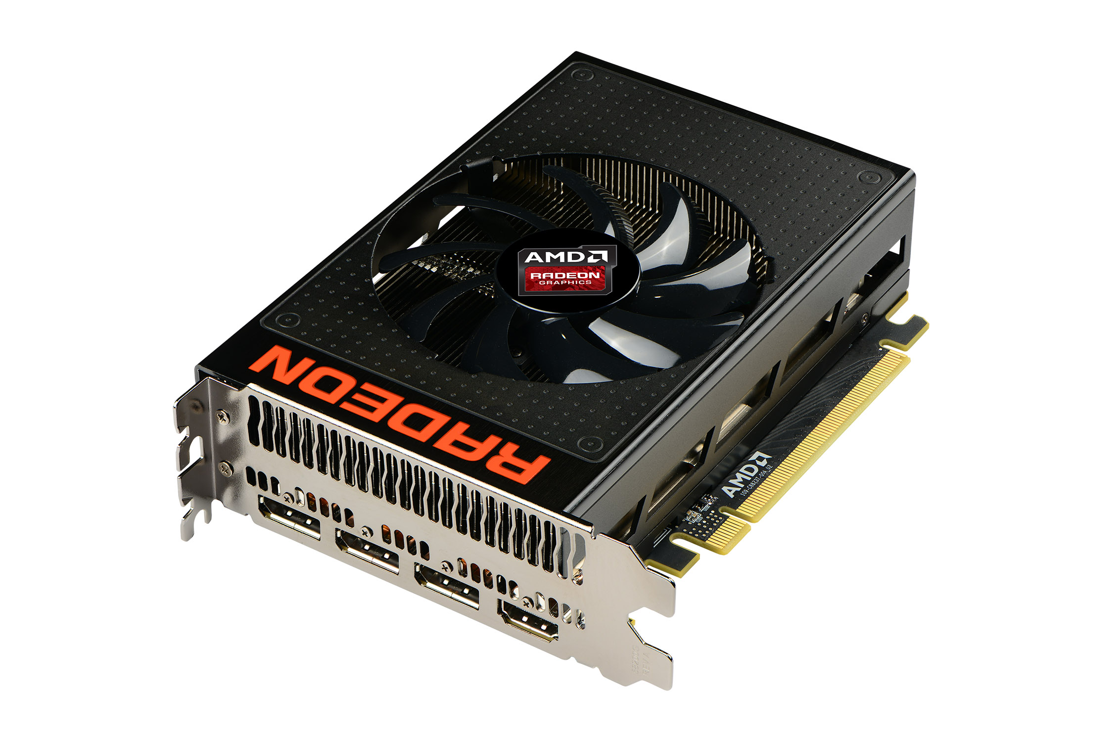
The overall design of the R9 Nano’s cooler is best described as a combination open-air and half-blower hybrid. The design is technically open-air, employing a single axial fan to cool the card. However with only a single fan AMD has been able to align the heatsink fins horizontally and then place the fan in the center of the heatsink. The end result is that roughly half of the heat produced by the card is vented outside of the case, similar to a full blower, while the other half of the heat is vented back into the case. This reduces (though doesn’t eliminate) the amount of hot air being recycled by the card.
The heatsink itself is composed of aluminum and runs virtually the entire length of the card. This is technical a two-piece heatsink, with the primary heatsink composing the bulk of the card, while a much smaller secondary heatsink it found towards the far end of the card and mounted on top of a heatpipe.
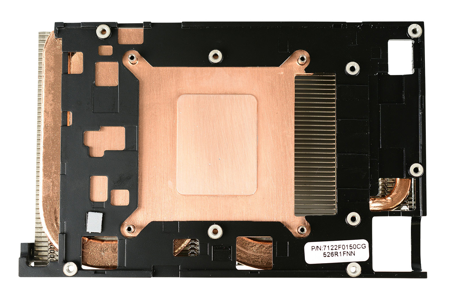
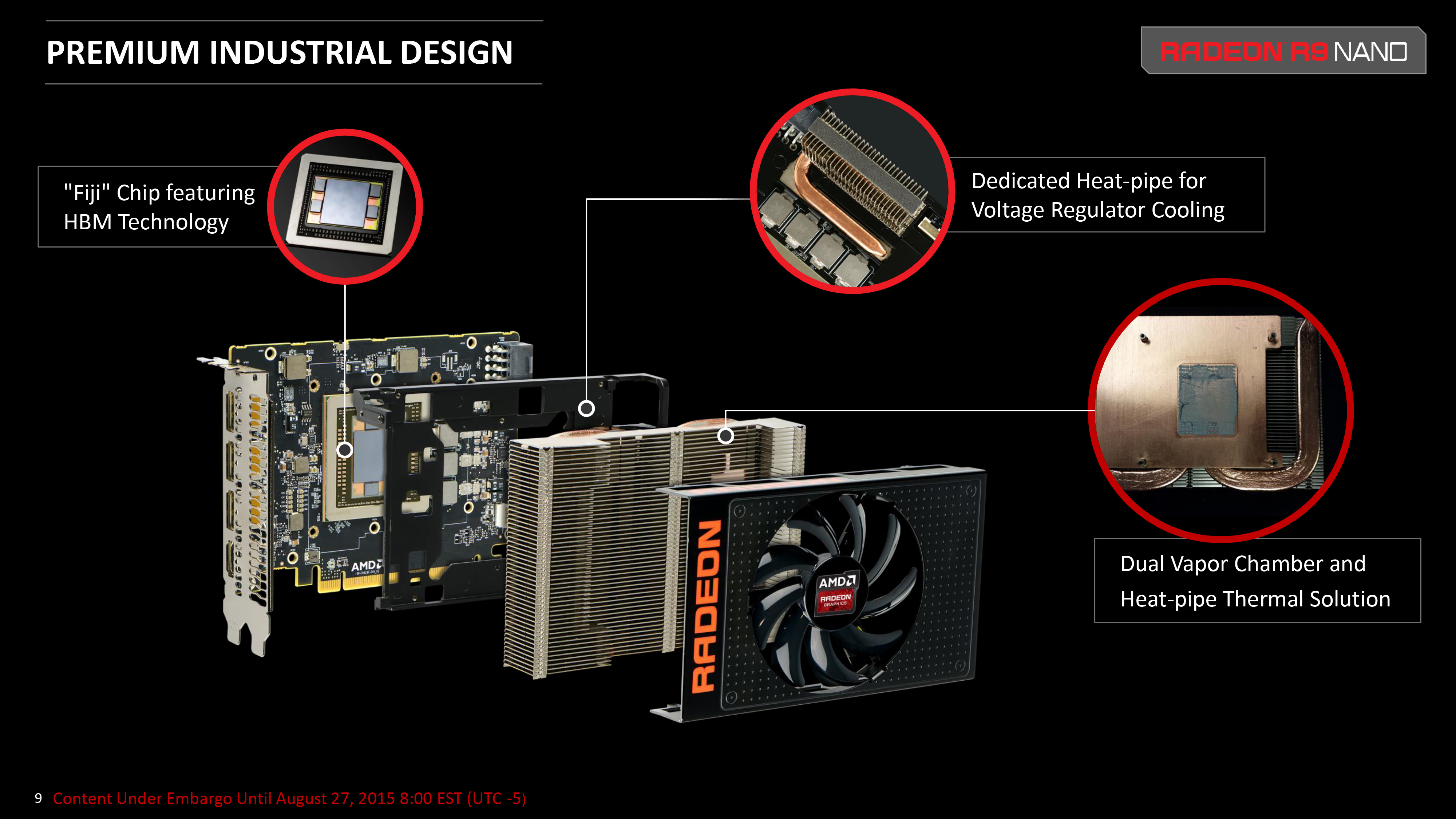
Drilling down, we find that the primary heatsink is fed by a combination vapor chamber and heatpipe design. A copper vapor chamber serves to draw heat away from the Fiji GPU and HBM stacks, and then heatpipes are used to better distribute heat to the rest of the heatsink. The use of a vapor chamber in the R9 Nano makes a lot of sense given the fact that vapor chambers are traditionally the most efficient heatsink base type, however the R9 Nano is also unique in that we typically don’t see vapor chambers and heatpipes used together. Other designs such as the high-end GeForce series use a single large vapor chamber across the entire heatsink base, so among reference cards at least the R9 Nano stands alone in this respect. In this case given AMD’s design goals for size and noise, a vapor chamber will play a big part in helping the small card effectively and quietly dissipate 175W.

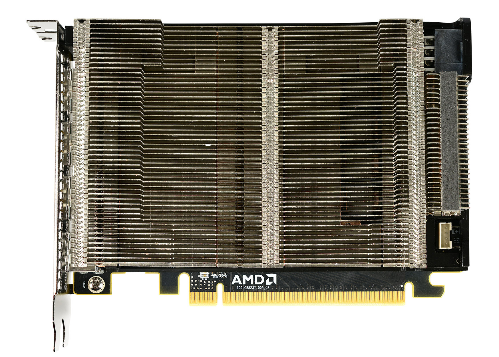
As for the physical PCB itself, as we can see AMD made it a relatively packed card in order to get the R9 Nano down to 6 inches. Compared to the R9 Fury X reference board, the biggest change here is that AMD has removed a fair bit of power circuitry to save space. By our count there are 4 VRM phases to feed the Fiji GPU, as opposed to the 6 found on R9 Fury X. Power delivery is handled by a single 8-pin PCIe power socket, which is becoming increasingly common, replacing the 2x 6-pin setup for 150W-225W cards.

Meanwhile to further shrink the overall PCB footprint, AMD has moved some of the remaining power delivery circuitry to the back of the card. The front of the card still contains the inductors and heat-sensitive MOSFETs, while a number of capacitors are on the rear of the card (and is why you won’t find a backplate).
Finally, for display I/O R9 Nano is unchanged from R9 Fury X. This means we’re looking at a DVI-free design, with 3x DisplayPort 1.2 and 1x HDMI 1.4 port all along a single row of the I/O bracket. Buyers looking to put together HTPCs will want to be especially mindful of the HDMI 1.4 port; while it's not necessarily a deal-breaker, it does mean that the R9 Nano can't fully drive 4Kp60 TVs, which are slowly but surely becoming more common.
Overall AMD is rather confident in their design for the R9 Nano. The heatsink is built to efficiently dissipate more heat than the 175W the card requires (despite the small size), and as a result we never see the R9 Nano thermally throttle under normal operation. The card’s thermal throttle point is 85C, and in our testing the card never passed 75C, exactly as AMD promised us. What ends up limiting the R9 Nano’s performance then is exactly as expected: the power throttling.


284 Comments
View All Comments
brikbot - Thursday, September 10, 2015 - link
*capacitor ;)tipoo - Thursday, September 10, 2015 - link
Nah, capacitors are the big cylindrical oneshttp://www.thenakedpc.com/dan/Bulging_Capacitors/c...
Resistors are the little ones scattered all over motherboards and other PCBs
https://www.google.ca/search?q=motherboard+resisto...
extide - Thursday, September 10, 2015 - link
No, those are capacitors. They are for decoupling for the GPU power rails, and that's why they have to be right under the GPU as it's as close to the chip as they can get.Furthermore, you can see the designations on the PCB are Cxxx indicating again that they are capacitors.
SMD resistors and capacitors can look identical. You are thinking of electrolytic capacitors (the big round ones) where as these are ceramic capacitors. Also the large black ones with a grey line on the side which are on the opposite side of the PCB relative to the MOSFETS are tantalum capacitors. There are MANY types.
However one rule of thumb that is not always true, but usually is, the tan colored small SMD devices are usually capacitors whereas black ones tend to be resistors, although I stress that this is not always the case. Best way to find out is look at the component designation on the board, if they start with C they are caps, and resistors will start with R.
brikbot - Friday, September 11, 2015 - link
This exactly. And a good example of an exception are film capacitors, which tend to be black.brikbot - Thursday, September 10, 2015 - link
Regarding power consumption for gaming vs FurMark: what impact could AMD's drivers be having? As in, we see cases where the AMD cards are CPU limited and nVidia's cards are not, implying that the AMD drivers drive a higher CPU load that nVidia. This would make sense in my mind with FurMark which loads the GPU down without really applying any loading on the CPU. I guess I'm wondering if the higher power load in gaming, being measured from the wall, is being driven by a higher CPU load as the drivers try to keep the GPU fed whereas in FurMark the drivers do not have the same work, letting the CPU idle, resulting in the lower power numbers.It might make an interesting metric to check in the future, given DX12 changing the impact of drivers.
slapdashbr - Friday, September 11, 2015 - link
Furmark draws substantially more power at a given clock speed than... anything else. It's like intel burn test. It's an unrealistic workload.Daniel Egger - Thursday, September 10, 2015 - link
"GTX 970 is also cheaper and designed to draw less power"Not true, for some stupid reason most mini GTX 970 draw more power and require 2 PCIe connectors.
extide - Thursday, September 10, 2015 - link
Requiring 2 connectors doesnt mean it draws more power, and they are probably 2x6pin which is rated for the same as 1x8pinDaniel Egger - Friday, September 11, 2015 - link
True, there's still the problem that a few mini PSUs only have 1x8 pin PCIe connector and the cards will not start if only one is connected. I'd rather not fool arounds with Y-adapters or other tricks at this amp-age; that can go south rather quickly...Daniel Egger - Thursday, September 10, 2015 - link
"And while we disagree that this card is suitable for 4K gaming based on its sub-Fury performance, we’re including 4K results anyhow to serve as a point of comparison."WTF is this? "And while we disagree that this car is suitable for racing based on its sub-911 GT3 RS performance, we’re including lap times anyway to serve as a point of comparison."