The Intel Skylake Mobile and Desktop Launch, with Architecture Analysis
by Ian Cutress on September 1, 2015 11:05 PM ESTWhat to Expect
With Intel going for a full YUHS launch today, looking up and down the stack there are a number of interesting things to consider at each segment. Starting with Skylake-Y, or Core M, the new branding to m7/m5/m3 will hopefully make it easier for users to ascertain the performance of their processor, but it also allows Intel to inject vPro into various SKUs, such as the upcoming update to Intel’s Compute Stick.
In the mini-PC space, through various sources in the industry, we are told that it is the vPro moniker for these devices (such as the NUC and Compute Stick) that generate the higher proportion of sales. At this point, the vPro versions of Core M are not due out until later in Q4/even Q1, but I assume we should see something at the Consumer Electronics Show during the first week of January.
One element we haven’t touched upon is how Intel will implement different TDP aspects to both its Skylake-Y and Skylake-U lines. With Haswell and Broadwell, most processors had a cTDP Up and a cTDP Down mode that allowed the device OEM to take a processor and move it slightly outside its normal TDP window, perhaps to take advantage of a chassis design they already had and either increase battery life or increase performance.
Now due to Speed Shift, one could argue that cTDP down is less relevant, and when cTDP up is available and a Speed Shift aware operating system is installed, that setting might be used as well. Because Speed Shift is not universal, there is still this element of cTDP Up and Down to contend with. To insert a few more caveats, it seems like SDP (scenario design power) might also be part of the equation, especially in the Skylake-Y domain.
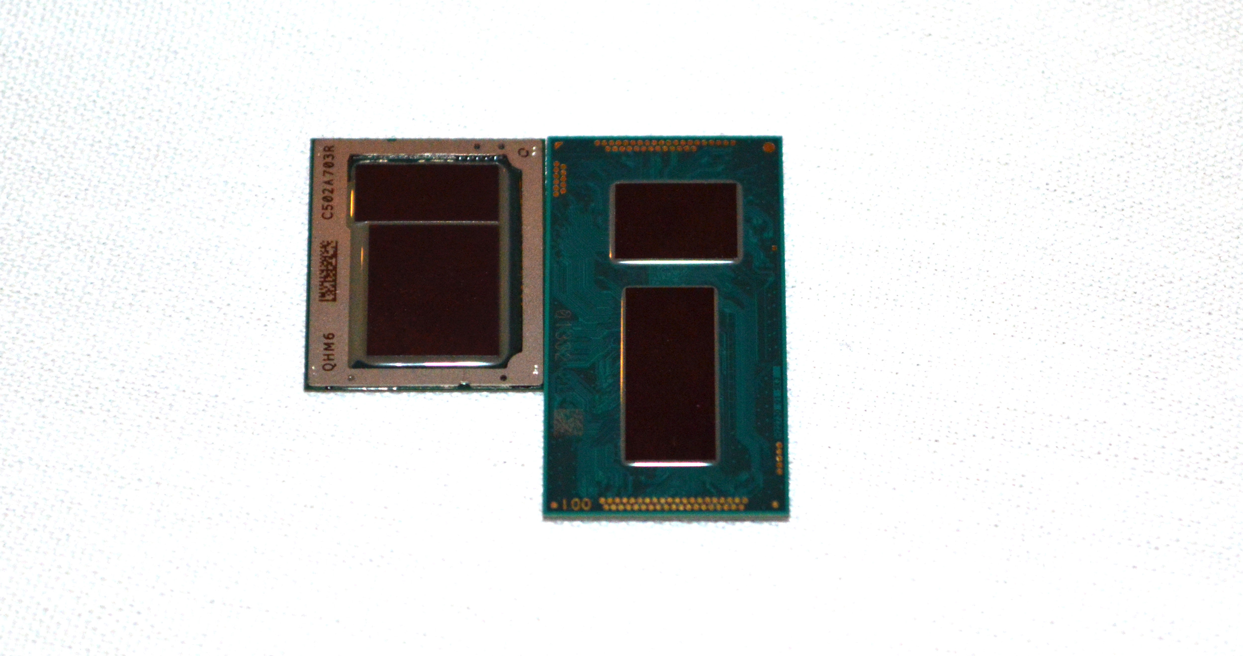
It is worth noting that the Skylake-Y package is crazy small. At IDF Intel showed off a finished Skylake-Y package to demonstrate the CPU die size in relation to the package size, and to compare the overall package size to the already small Broadwell-Y package. While both packages are still 16.5mm wide, Intel has compacted the overall layout and squared off the CPU die, bringing the height of the Skylake-Y package down from 30mm to 20mm, a 33% savings in package size.
Meanwhile Intel also had the other BGA Skylake processor packages on display as well:

Actually in this shot, we can calculate the die size of the Y 2+2 die to be approximately 98.5 mm2 (9.57mm x 10.3mm). This is compared to the 4+2 arrangement on Skylake-K which we measured at 122.4mm2. At this package size of 20 x 16.5 mm, Intel is claiming a 40% gain in graphics performance for Skylake-Y over Broadwell-Y, which will be interesting to compare when we get some samples in house.
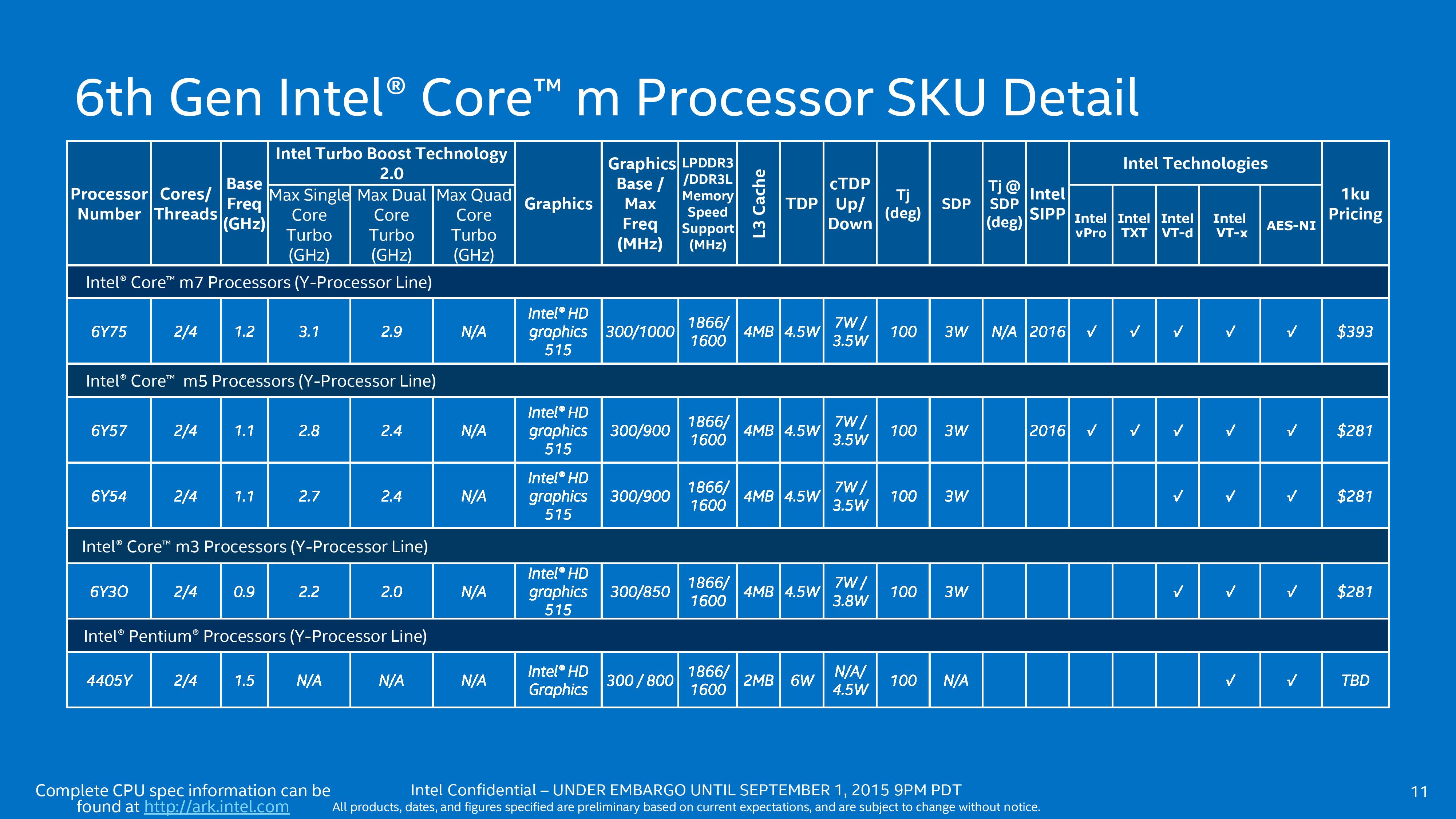
Skylake-Y still comes in as Intel’s premium low power processor, with 1K pricing from $281 to $393. That more or less aligns with Broadwell-Y, but we also get a Pentium model that is severely cut with no turbo mode and only 1 MB of L3 cache per core.
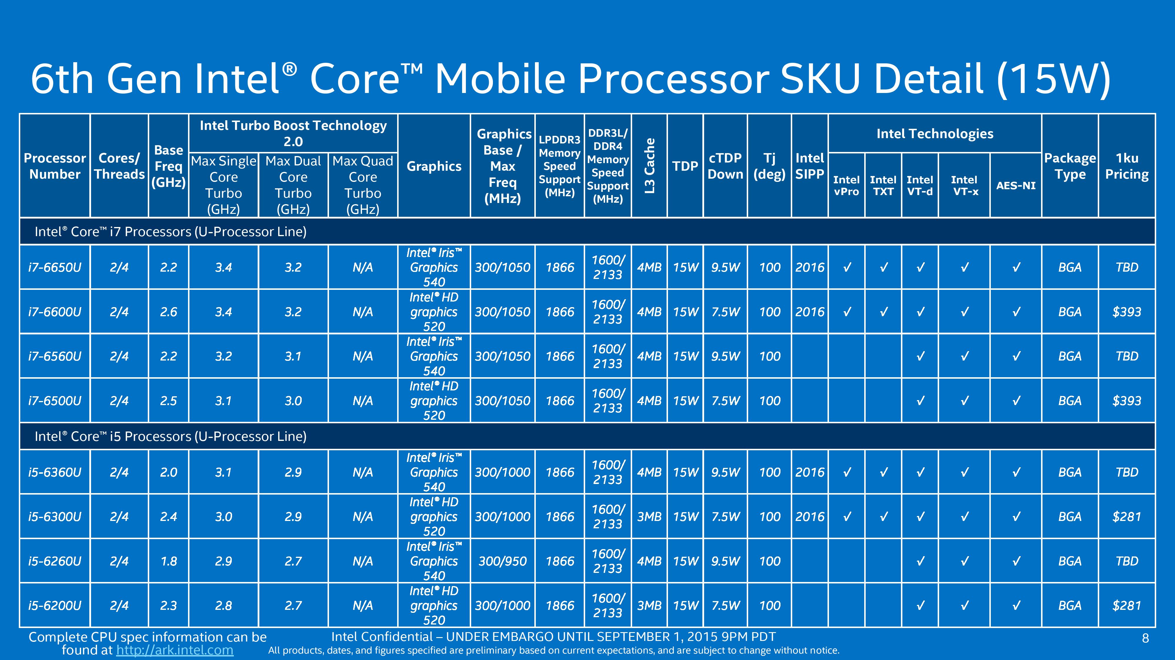
The 15W models of Skylake-U either follow the 00U naming for GT2 graphics (24 EUs) or 50U/60U for GT3e graphics (48 EUs with 64MB eDRAM). The pricing on the GT3e parts is not given as they will be coming later in the year, but it can be pointed out that the base frequency for the GT2 parts is actually higher than the GT3 parts. Also, the L3 cache on the i5-U processors with GT2 is at 1.5 MB/core rather than 2 MB/core. Normally all the i5 parts would be below the i7 parts, but because the eDRAM arrangement moves up to 2 MB/core, the i5-U parts with GT3e have to comply.
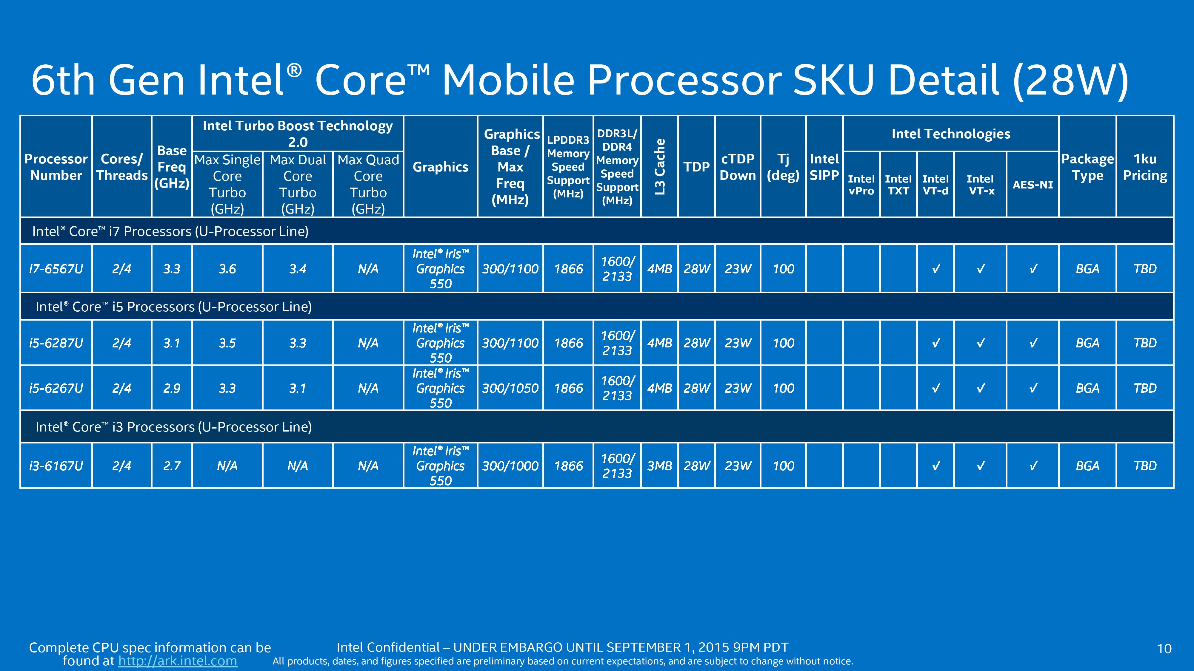
Moving up to 28W with Skylake-U presents us with the higher power GT3e models. Similarly, the pricing has not been announced for these but for all the processors the base frequency is relatively high (2.7 GHz to 3.3 GHz) with only a small jump to the maximum frequency. The i3 at the bottom without any turbo frequency but with GT3e would be an interesting part to play with.
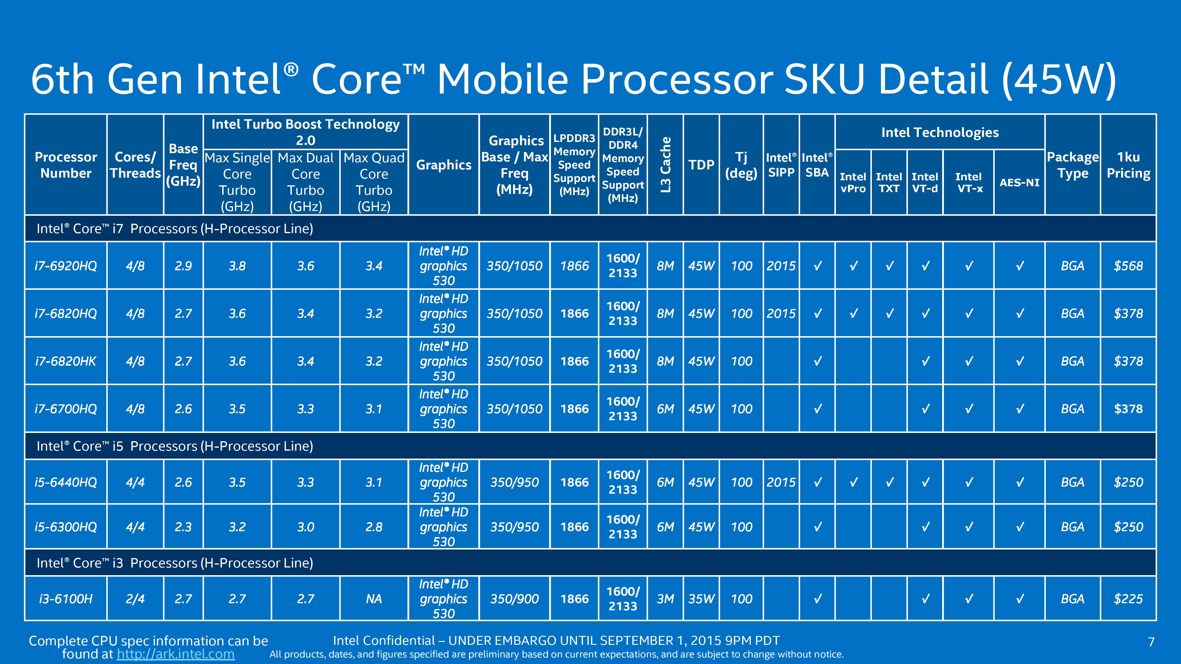
At 45W, the Skylake-H mobile processors almost all move into quad core territory here, aligning with the power increase, but also moving down to GT2 arrangements. We get a vew vPro enabled parts here too, and the pricing of the i5 seems quite reasonable.
There is one part that stands out – the i7-6820HK. This is Intel’s mobile part that can be user overclocked. Yes, that’s not a typo. This processor is designed to go into laptop systems that have sufficient cooling (either high powered air… or water) and can be pushed when they are needed. Expect to see this part in the large 17” desktop replacement gaming systems over the next few months.
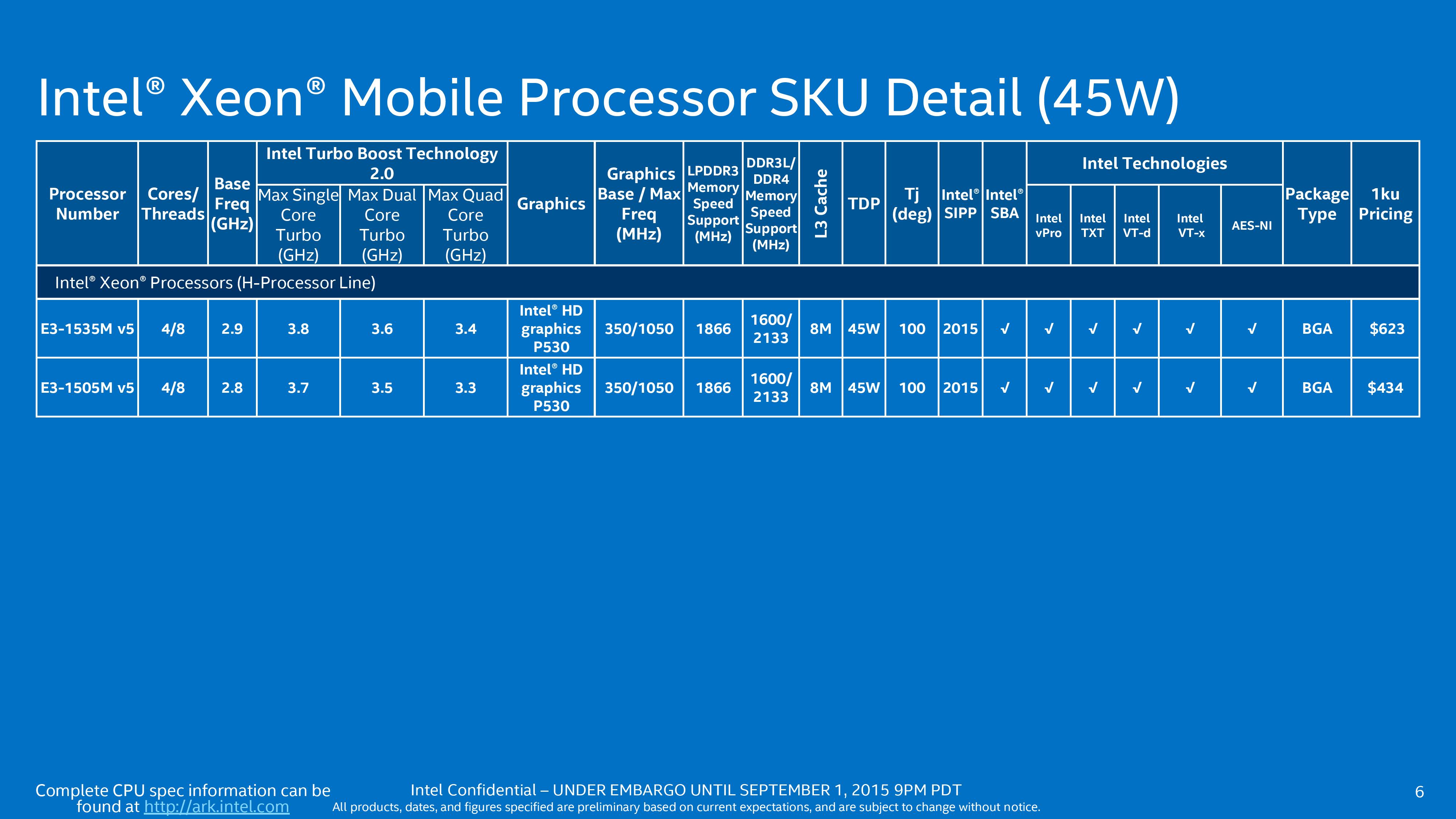
Intel is also releasing a couple of mobile processors under the Xeon branding. This means ECC support and all the other Xeon benefits, but in a processor specifically designed for notebooks rather than a repurposed desktop processor that might not fit properly / give the best ergonomics. When these were announced, it was perhaps wishful thinking that Xeon would come down to 15W, perhaps offering ultrabooks with this feature set, though I imagine at 45W we will see some desktop-replacement workstations with professional grade graphics cards, such as the already-announced Lenovo workstation laptops.
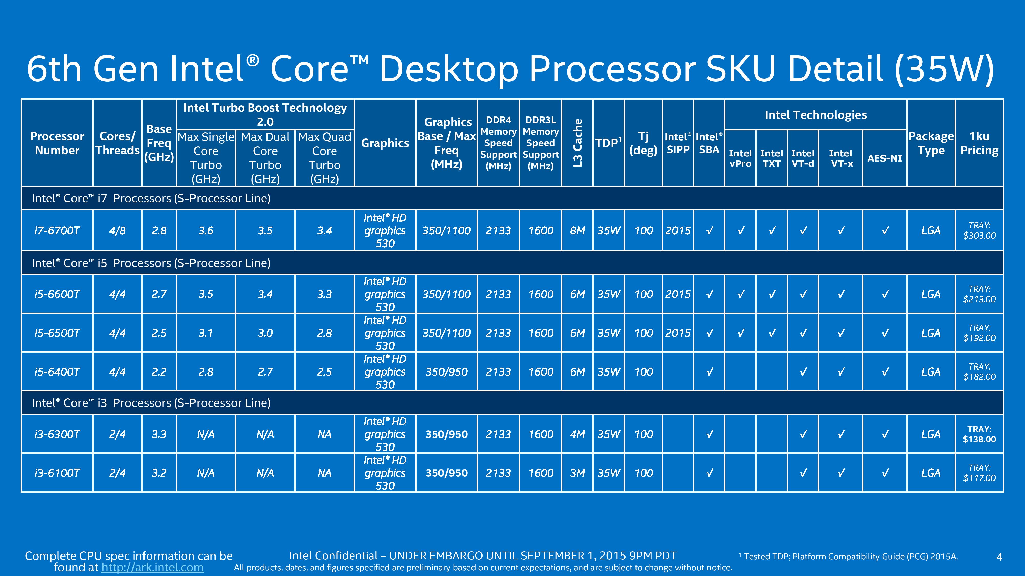
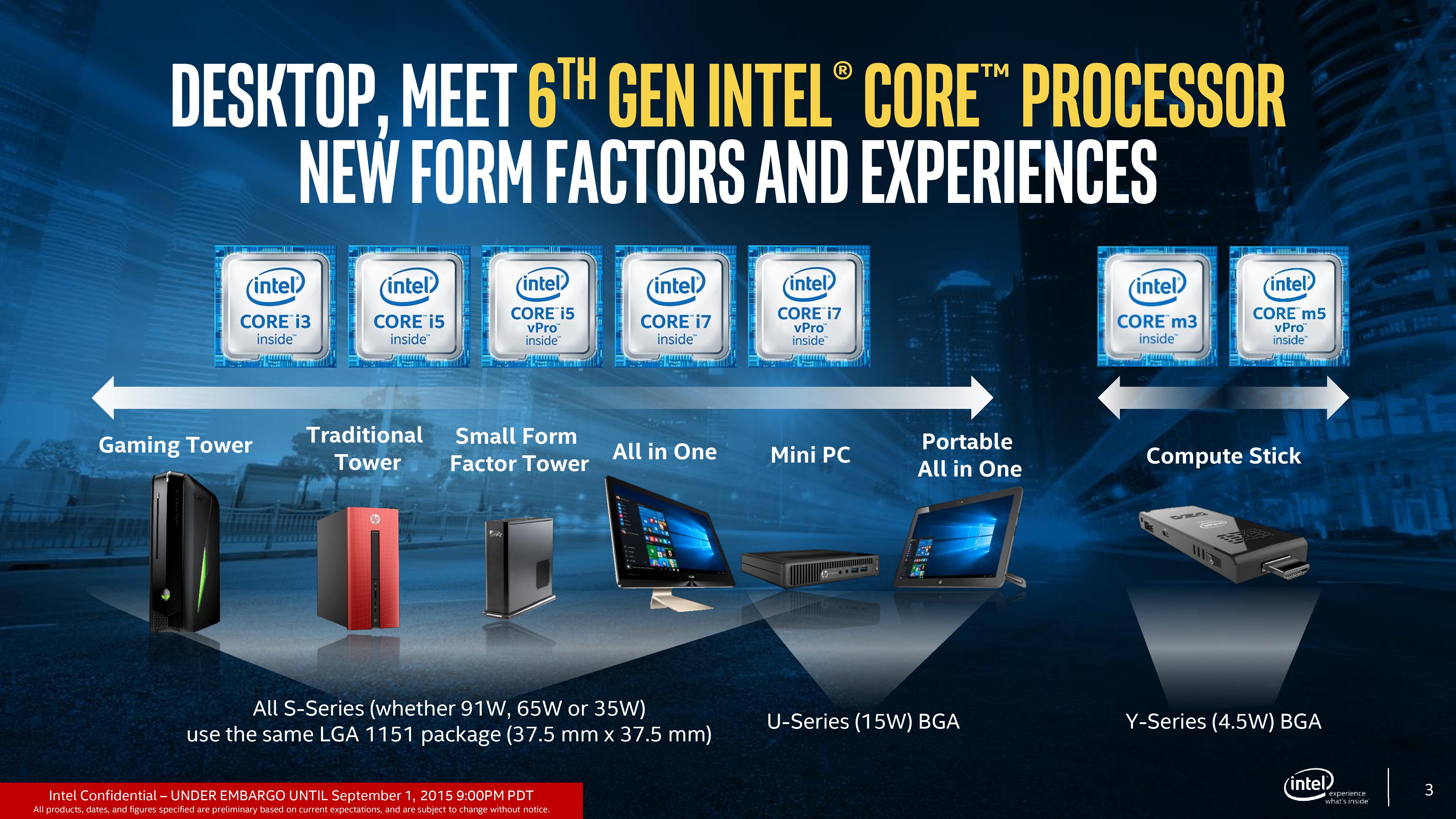
On the Skylake-S side of the equation, the processors come in two segments. Here is the list of the low powered processors that have the ‘T’ in the name, or unofficially known as ‘Skylake-T’. These are all 35W, some with vPro, but covering the i3/i5/i7 lines sufficiently.

The non-T and non-K desktop processors come in at 65W, and there are no real surprises here in the product lines as they migrate well enough from previous generation designations. All the Skylake-S i3/i5/i7 processors have HD 530 graphics.
Beyond Skylake and to Kaby Lake
Post Skylake, Intel is breaking from the tick-model to tick-tock-tock, posting a third generation on 14nm called Kaby Lake (pronounced Kah-bee, as far as we were told).
This stems from the issues of moving to smaller process nodes. At 14nm, this equates to only 90 silicon atoms, meaning ever more intensive manufacturing is required which drives up cost and reduces yield. Due to the issues Intel had at 14nm using their second generation FinFET method and more advanced double patterning, initial costs were high and yields were lower than expected for the timeframe, pushing Broadwell to a later-than-expected timeline. Skylake was kept to the regular timeline, resulting in a brief outing for Broadwell (on the desktop especially). But we suspect that similar reasoning is behind a delay from 14nm to 10nm –more esoteric ways under conventional methodology are required to keep driving the node down, and with that comes extra challenges that delay both time to market and yield numbers before tweaking the design.
We’ve mentioned in the past that the development of extreme-ultra-violet (EUV) technology is one element that could assist this drive down, however Intel is not expected to implement this for 10nm but rather for 7nm, which is still several years down the road. To that end, tick-tock is not dead, but merely stretching out.


173 Comments
View All Comments
Xenonite - Thursday, September 3, 2015 - link
Actually, it seems that power consumption is the only thing that matters to consumers, even on the desktop.All this talk about AMD's lack of competition being the reason why we aren't seeing meaningful generational performance improvements is just that: talk.
The real thing that hampers performance progress is consumers' plain refusal to upgrade for performance reasons (even a doubling in performance is not economically viable to produce since no one, except for me it seems, will buy it).
Consumers only buy the lowest power system that they can afford. It has nothing to do with AMD.
Even if AMD released a CPU that is 4x faster than piledriver, it wouldn't change Intel's priority (nor would it help AMD's sales...).
IUU - Wednesday, September 2, 2015 - link
Sorry for my tone , but "I'm failing to see", how transistor count don't mean more to consumers than to anyone else.So, after 10 years of blissful carelessness(because duuude it's user experience dat matters, ugh..),
you will have everyone deceiving you on what they offer on the price point they offer. Very convenient, especially if they are not able to sustain an exponential increase in performance and passing to the next paradigm to achieve it.
Because untill very recently we have been seeing mostly healthy practices, despite the fact that you could always meet people pointing to big or small sins.
Big example, What's the need of an igp on a processor that consumes 90 watts, especially a gpu that is tragically subpar? To hide the fact they have nothing more to offer to the consumer, cpu dependent, at 90 watts(at the current market situation) and have an excuse for charging more on a
theoretically higher consuming and "higher performing" cpu?
Because, what bugs me is what if 6700k lacked the igp? Would it perform better without a useless igp dragging it down? I really don't know, but I feel it wouldn't.
Regarding the mobile solutions and the money and energy limited devices, the igp could really prove to be useful to a lot of people, without overloading their device with a clunky, lowly, discrete gpu.
xenol - Wednesday, September 2, 2015 - link
If the 6700K lacked the iGPU with no other modifications, it would perform exactly the same.MrSpadge - Wednesday, September 2, 2015 - link
Yes, it would perform exaclty the same (if the iGPU is not used, otherwise it needs memory bandwidth). But the chip would run hotter since it would be a lot smaller. Si is not the best thermal conductor, but the presence of the iGPU spreads the other heat producers a bit.xenol - Wednesday, September 2, 2015 - link
I don't think that's how thermals in ICs work...MrSpadge - Wednesday, September 2, 2015 - link
Thermodynamics "work" and don't care if they're being applied to an IC or a metal brick. Silicon is a far better heat conductor than air, so even if the GPU is not used, it will transfer some of the heat from the CPU + Uncore to the heat spreader.My comment was a bit stupid, though, in the way that given how tightly packed the CPU cores and the uncore are, the GPU spreads none of them further apart from each other. It could have been designed like that, but according to the picture on one of first few pages it's not.
Xenonite - Thursday, September 3, 2015 - link
No, it wouldn't. You could easily spread out the cores by padding them with much more cache and doubling their speculative and parallel execution capabilities. If you up the power available for such out of order execution, the additional die space could easily result in 50% more IPC throughput.MrSpadge - Thursday, September 3, 2015 - link
50% IPC increase? Go ahead and save AMD, then! They've been trying that for years with probably billions of R&D budget (accumulated over the years), yet their FX CPUs with huge L3 don't perform significantly better than the APUs with similar CPU cores and no L3 at all.Xenonite - Thursday, September 3, 2015 - link
Yes, but I specifically mentioned using that extra cache to feed the greater amount of speculative execution units made available by the removal of the iGPU.Sadly, AMD can't use this strategy because Global Foundaries' and TSMC's manufacturing technology cannot fit the same amount of transistors into a given area, as Intel's can.
Furthermore, their yields for large dies are also quite a bit lower and AMD really doesn't have the monetary reserves to produce such a high-risk chip.
Also, the largest fraction of that R&D budget went into developing smaller, cheaper and lower power processors to try and enter the mobile market, while almost all of the rest went into sacrificing single threaded design (such as improving and relying more on out of order execution, branch prediction and speculative execution) to design Bulldozer-like, multi-core CPUs (which sacrifice a large portion of die area, that could have been used to make a low amount of very fast cores, to implement a large number of slow cores).
Lastly, I didn't just refer to L3 cache when I suggested using some of the free space left behind by the removal of the iGPU to increase the amount of cache. The L1 and L2 caches could have been made much larger, with more associativity to further reduce the amount and duration of pipeline stalls, due to not having a data dependancy in the cache.
Also, while it is true that the L3 cache did not make much of a difference in the example you posted, its also equally true that cache performance becomes increasingly important as a CPU's data processing throughput increases.
Modern CPU caches just seem to have stagnated (aside from some bandwidth inprovements every now and then), because our CPU cores haven't seen that much of a performance upgrade since the last time the caches have been improved.
Once a CPU gets the required power and transistor budgets for improved out of order performance, the cache will need to be large enough to hold all the different datasets that a single core is working on at the same time (which is not a form a multi-threading in case you were wondering), while also being fast enough to service all of those units at once, without adversely affecting any one set of calculations.
techguymaxc - Wednesday, September 2, 2015 - link
Your representation of Skylake's CPU/IPC performance is inaccurate and incomplete due to the use of the slowest DDR4 memory available. Given the nature of DDR4 (high bandwidth, high latency), it is an absolute necessity to pair the CPU with high clockspeed memory to mitigate the latency impairment. Other sites have tested with faster memory and seen a much larger difference between Haswell and Skylake. See Hardocp's review, (the gaming section specifically) as well as Techspot's review (page 13, memory speed comparison). Hardocp shows Haswell with 1866 RAM is actually faster than Skylake with 2133 RAM in Unigine Heaven and Bioshock Infinite @ lowest quality settings (to create a CPU bottleneck). I find Techspot's article particularly interesting in that they actually tested both platforms with fast RAM. In synthetic testing (Sandra 2015) Haswell with 2400 DDR3 has more memory bandwidth than Skylake with 2666 DDR4, it is not until you pair Skylake with 3000 DDR4 that it achieves more memory bandwidth than Haswell with 2400 DDR3. You can see here directly the impact that latency has, even on bandwidth and not just overall performance. Furthermore in their testing, Haswell with 2400 RAM vs. Skylake with 3000 RAM shows Haswell being faster in Cinebench R15 multi-threaded test (895 vs. 892). Their 7-zip testing has Haswell leading both Skylake configurations in a memory-bound workload (32MB dictionary) in terms of instructions per second. Finally, in a custom Photoshop workload Haswell's performance is once again sandwiched between the two Skylake configurations.Clearly both Haswell and Skylake benefit from faster memory. In fact, Skylake should ideally be paired with > 3000 DDR4 as there are still scenarios in which it is slower than Haswell with 2400 DDR3 due to latency differences.
Enthusiasts are also far more likely to buy faster memory than the literal slowest memory available for the platform, given the minimal price difference. Right now on Newegg one can purchase a 16GB DDR3 2400 kit (2x8) for $90, a mere $10 more than an 1866 16GB kit. With DDR4 the situation is only slightly worse. The cheapest 16GB (2x8) 2133 DDR4 kit is $110, and 3000 goes for $135. It is also important to note that these kits have the same (primary) timings with a CAS latency of 15.
So now we come to your reasoning for pairing Skylake with such slow RAM, and that of other reviewers, as you are not the only one to have done this. Intel only qualified Skylake with DDR4 up to 2133 MT/s. Why did they do this? To save time and money during the qualification stage leading up to Skylake's release. It is not because Skylake will not work with faster RAM, there isn't an unlocked Skylake chip in existence that is incapable of operating with at least 3000 RAM speed, and some significantly higher. Hardocp was able to test their Skylake sample (with no reports of crashing or errors) with the fastest DDR4 currently available today, 3600 MT/s. I have also heard anecdotally from enthusiasts with multiple samples that DDR4 3400-3600 seems to be the sweet spot for memory performance on Skylake.
In conclusion, your testing method is improperly formed, when considered from the perspective of an enthusiast whose desire is to obtain the most performance from Skylake without over-spending. Now, if you believe your target audience is not in fact the PC enthusiast but instead a wider "mainstream" audience, I think the technical content of your articles easily belies this notion.