The Intel Skylake Mobile and Desktop Launch, with Architecture Analysis
by Ian Cutress on September 1, 2015 11:05 PM ESTWhat to Expect
With Intel going for a full YUHS launch today, looking up and down the stack there are a number of interesting things to consider at each segment. Starting with Skylake-Y, or Core M, the new branding to m7/m5/m3 will hopefully make it easier for users to ascertain the performance of their processor, but it also allows Intel to inject vPro into various SKUs, such as the upcoming update to Intel’s Compute Stick.
In the mini-PC space, through various sources in the industry, we are told that it is the vPro moniker for these devices (such as the NUC and Compute Stick) that generate the higher proportion of sales. At this point, the vPro versions of Core M are not due out until later in Q4/even Q1, but I assume we should see something at the Consumer Electronics Show during the first week of January.
One element we haven’t touched upon is how Intel will implement different TDP aspects to both its Skylake-Y and Skylake-U lines. With Haswell and Broadwell, most processors had a cTDP Up and a cTDP Down mode that allowed the device OEM to take a processor and move it slightly outside its normal TDP window, perhaps to take advantage of a chassis design they already had and either increase battery life or increase performance.
Now due to Speed Shift, one could argue that cTDP down is less relevant, and when cTDP up is available and a Speed Shift aware operating system is installed, that setting might be used as well. Because Speed Shift is not universal, there is still this element of cTDP Up and Down to contend with. To insert a few more caveats, it seems like SDP (scenario design power) might also be part of the equation, especially in the Skylake-Y domain.
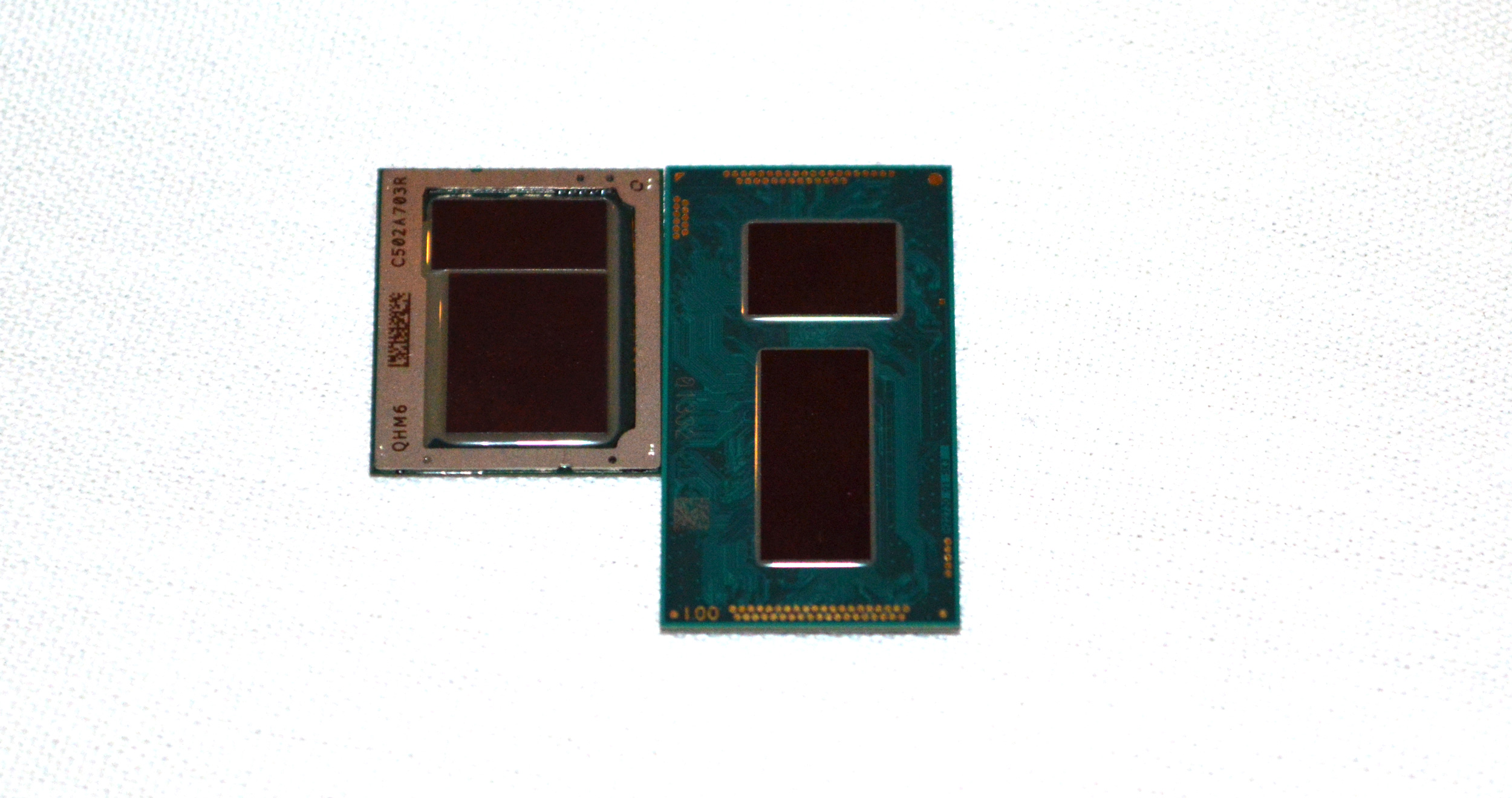
It is worth noting that the Skylake-Y package is crazy small. At IDF Intel showed off a finished Skylake-Y package to demonstrate the CPU die size in relation to the package size, and to compare the overall package size to the already small Broadwell-Y package. While both packages are still 16.5mm wide, Intel has compacted the overall layout and squared off the CPU die, bringing the height of the Skylake-Y package down from 30mm to 20mm, a 33% savings in package size.
Meanwhile Intel also had the other BGA Skylake processor packages on display as well:

Actually in this shot, we can calculate the die size of the Y 2+2 die to be approximately 98.5 mm2 (9.57mm x 10.3mm). This is compared to the 4+2 arrangement on Skylake-K which we measured at 122.4mm2. At this package size of 20 x 16.5 mm, Intel is claiming a 40% gain in graphics performance for Skylake-Y over Broadwell-Y, which will be interesting to compare when we get some samples in house.
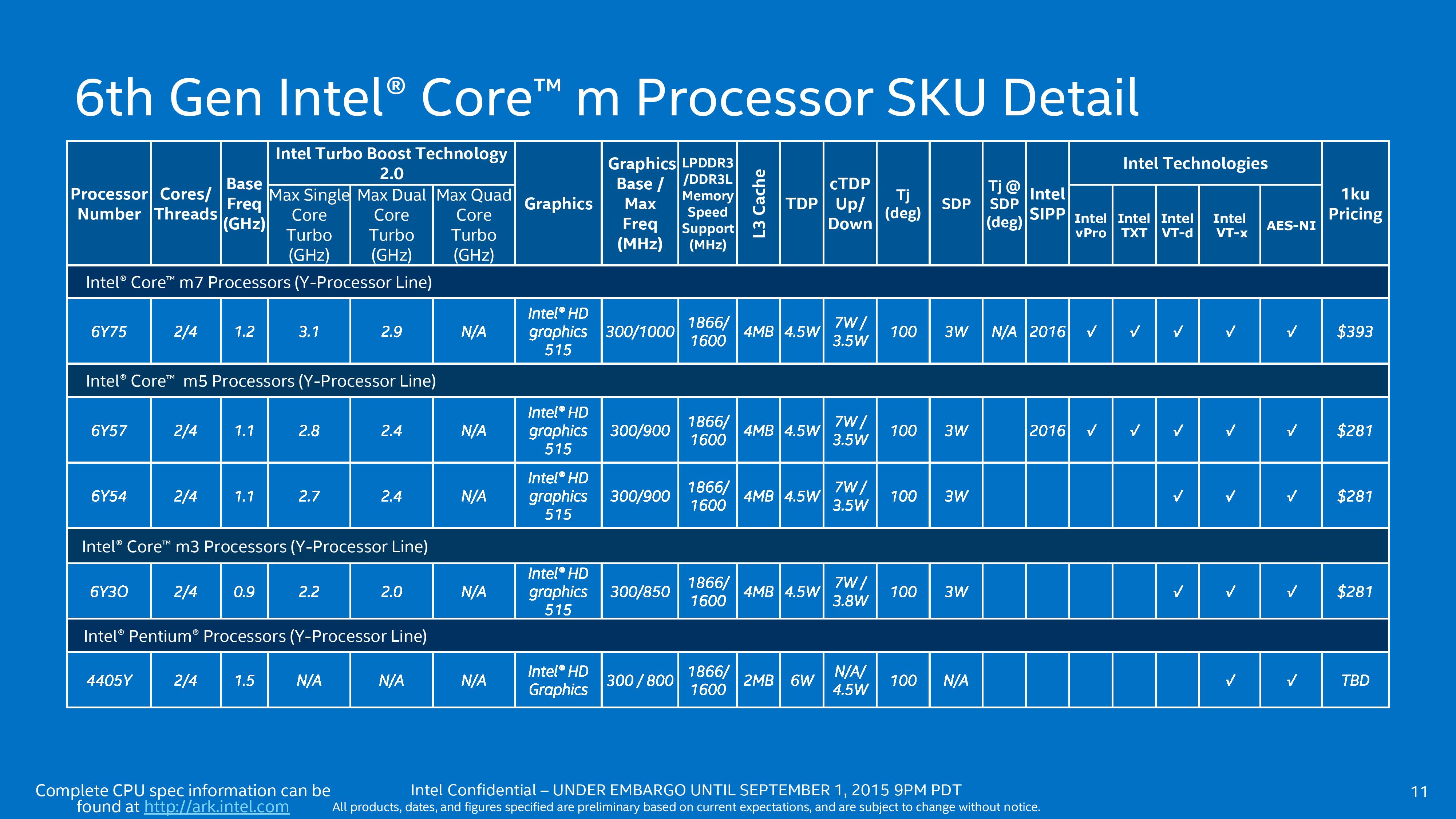
Skylake-Y still comes in as Intel’s premium low power processor, with 1K pricing from $281 to $393. That more or less aligns with Broadwell-Y, but we also get a Pentium model that is severely cut with no turbo mode and only 1 MB of L3 cache per core.
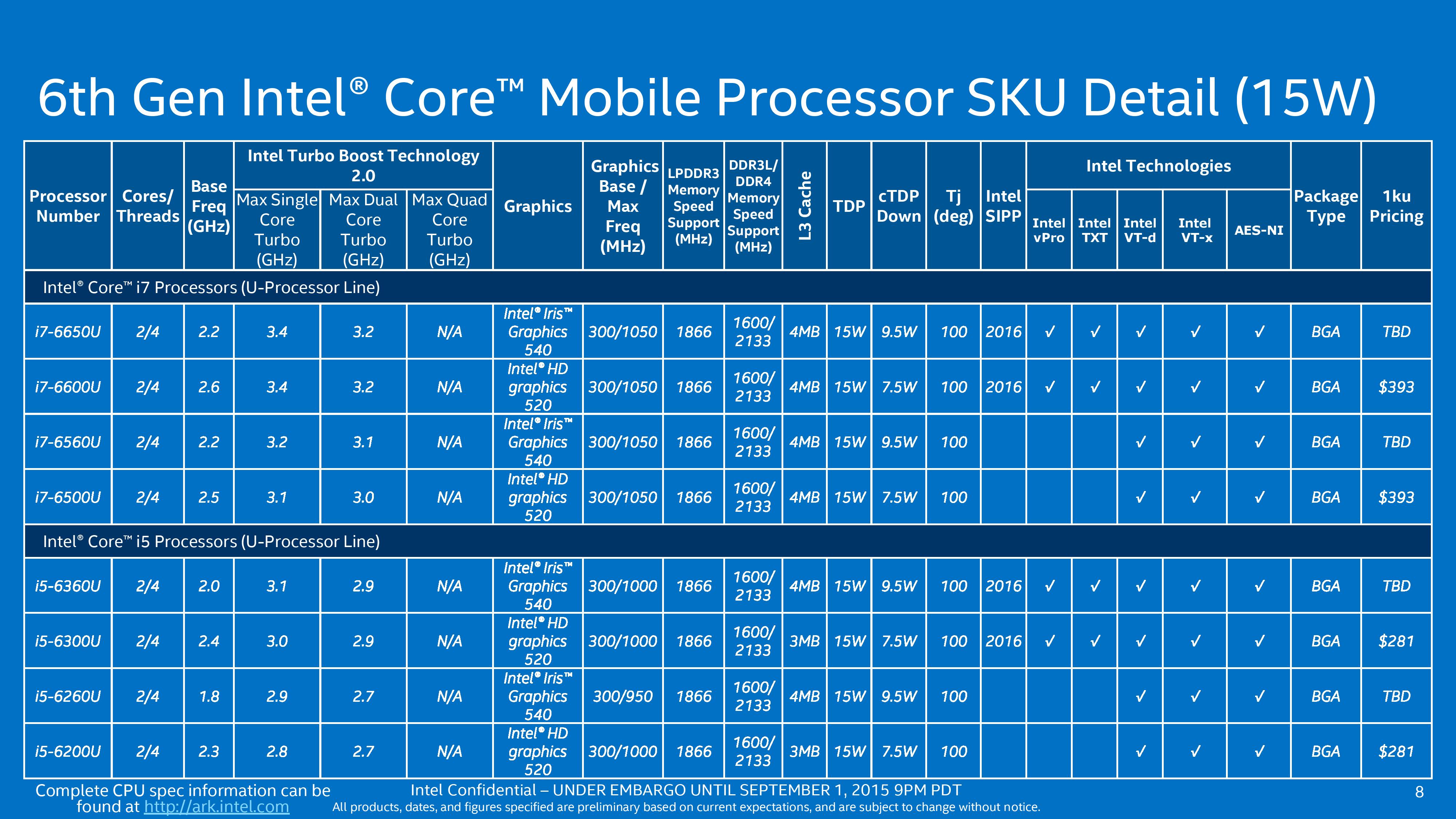
The 15W models of Skylake-U either follow the 00U naming for GT2 graphics (24 EUs) or 50U/60U for GT3e graphics (48 EUs with 64MB eDRAM). The pricing on the GT3e parts is not given as they will be coming later in the year, but it can be pointed out that the base frequency for the GT2 parts is actually higher than the GT3 parts. Also, the L3 cache on the i5-U processors with GT2 is at 1.5 MB/core rather than 2 MB/core. Normally all the i5 parts would be below the i7 parts, but because the eDRAM arrangement moves up to 2 MB/core, the i5-U parts with GT3e have to comply.
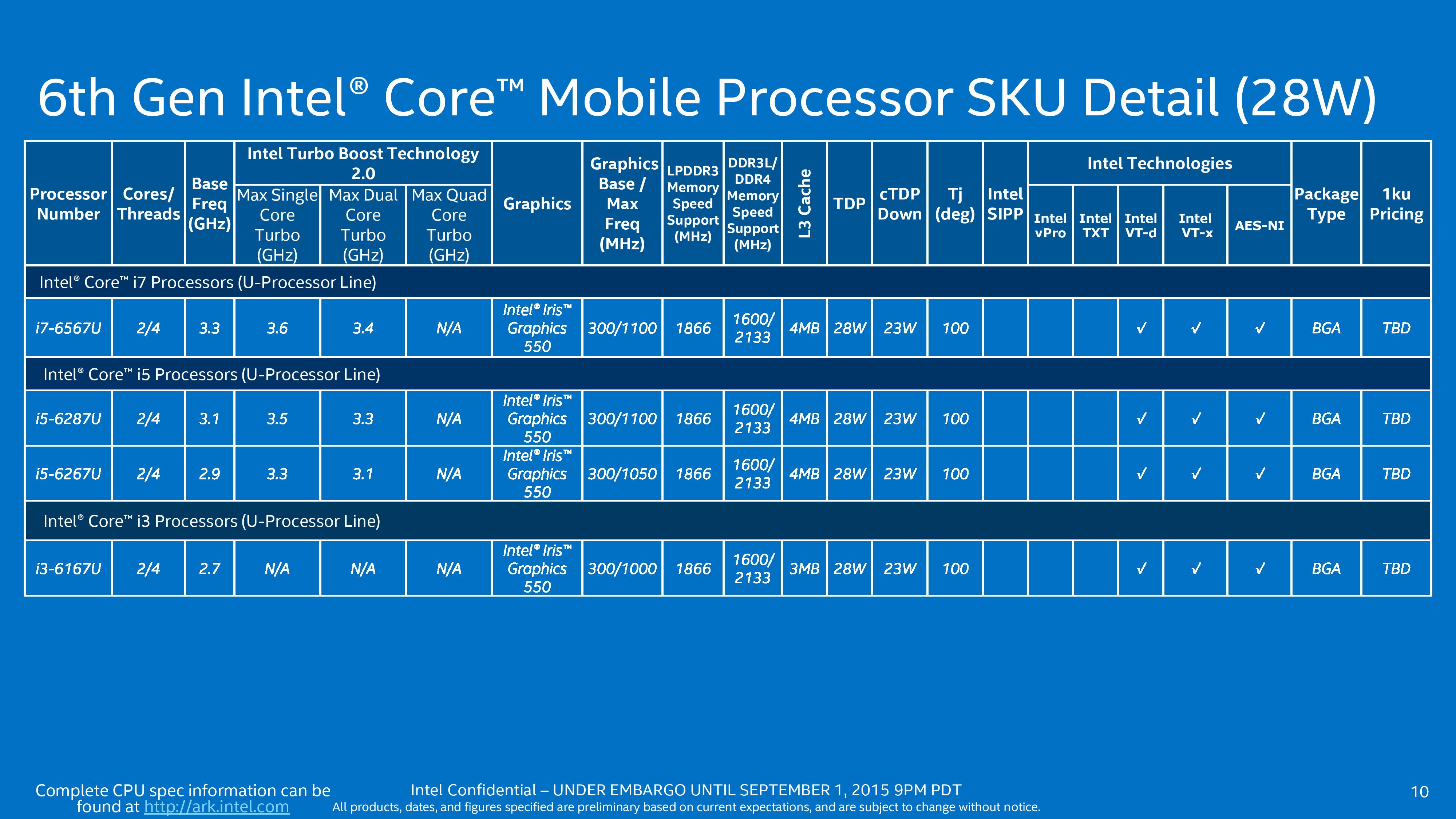
Moving up to 28W with Skylake-U presents us with the higher power GT3e models. Similarly, the pricing has not been announced for these but for all the processors the base frequency is relatively high (2.7 GHz to 3.3 GHz) with only a small jump to the maximum frequency. The i3 at the bottom without any turbo frequency but with GT3e would be an interesting part to play with.
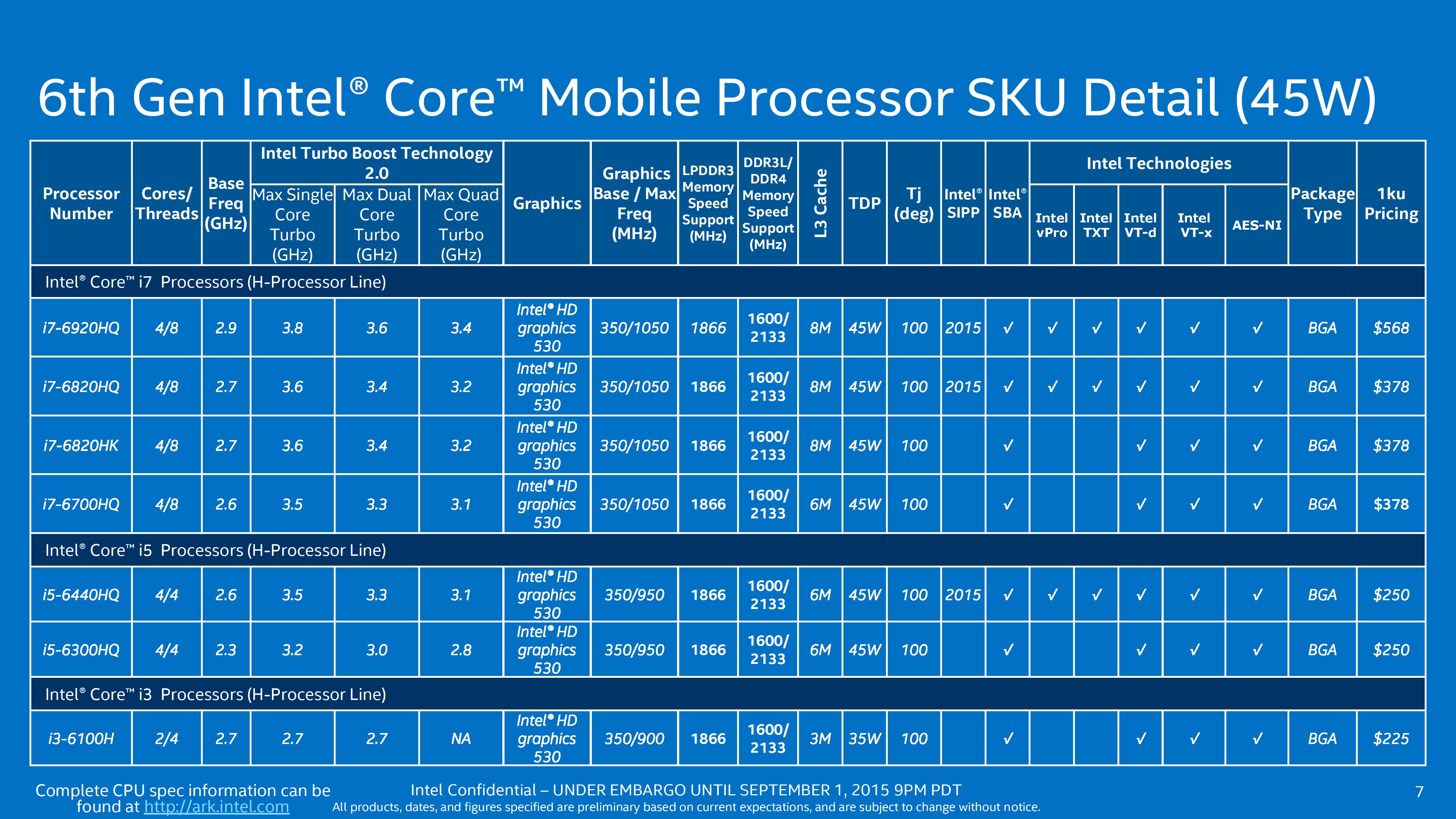
At 45W, the Skylake-H mobile processors almost all move into quad core territory here, aligning with the power increase, but also moving down to GT2 arrangements. We get a vew vPro enabled parts here too, and the pricing of the i5 seems quite reasonable.
There is one part that stands out – the i7-6820HK. This is Intel’s mobile part that can be user overclocked. Yes, that’s not a typo. This processor is designed to go into laptop systems that have sufficient cooling (either high powered air… or water) and can be pushed when they are needed. Expect to see this part in the large 17” desktop replacement gaming systems over the next few months.
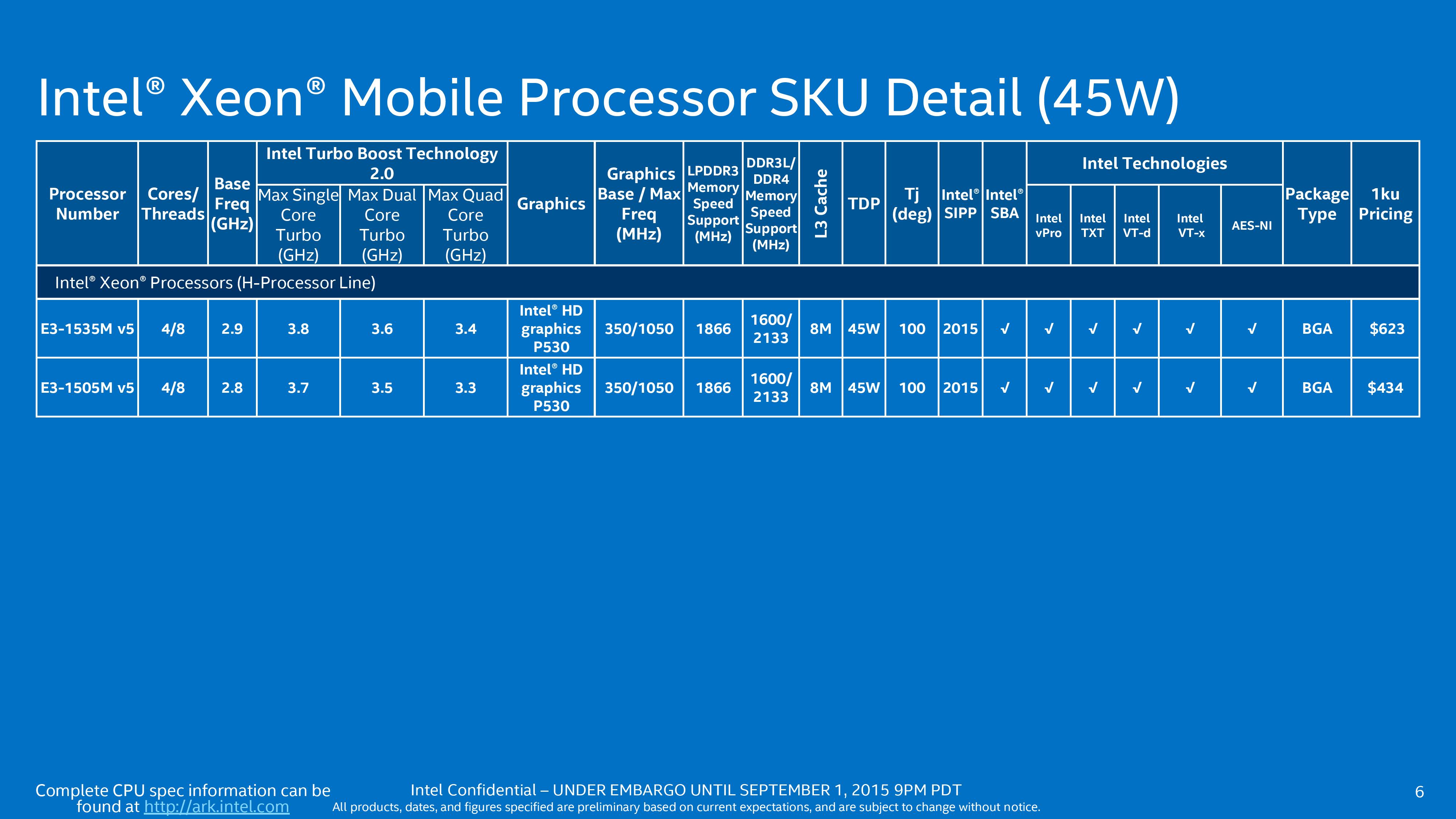
Intel is also releasing a couple of mobile processors under the Xeon branding. This means ECC support and all the other Xeon benefits, but in a processor specifically designed for notebooks rather than a repurposed desktop processor that might not fit properly / give the best ergonomics. When these were announced, it was perhaps wishful thinking that Xeon would come down to 15W, perhaps offering ultrabooks with this feature set, though I imagine at 45W we will see some desktop-replacement workstations with professional grade graphics cards, such as the already-announced Lenovo workstation laptops.
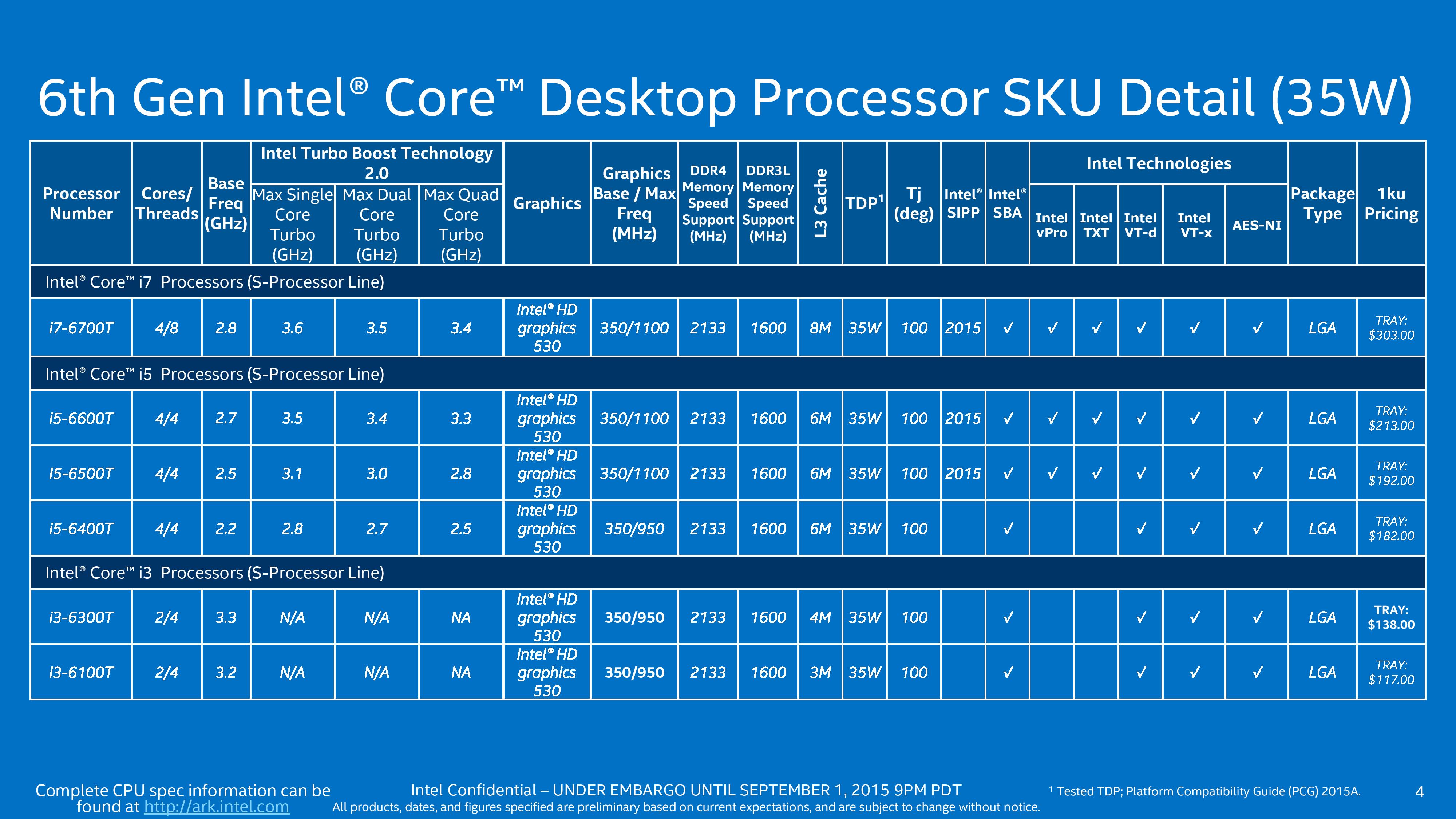
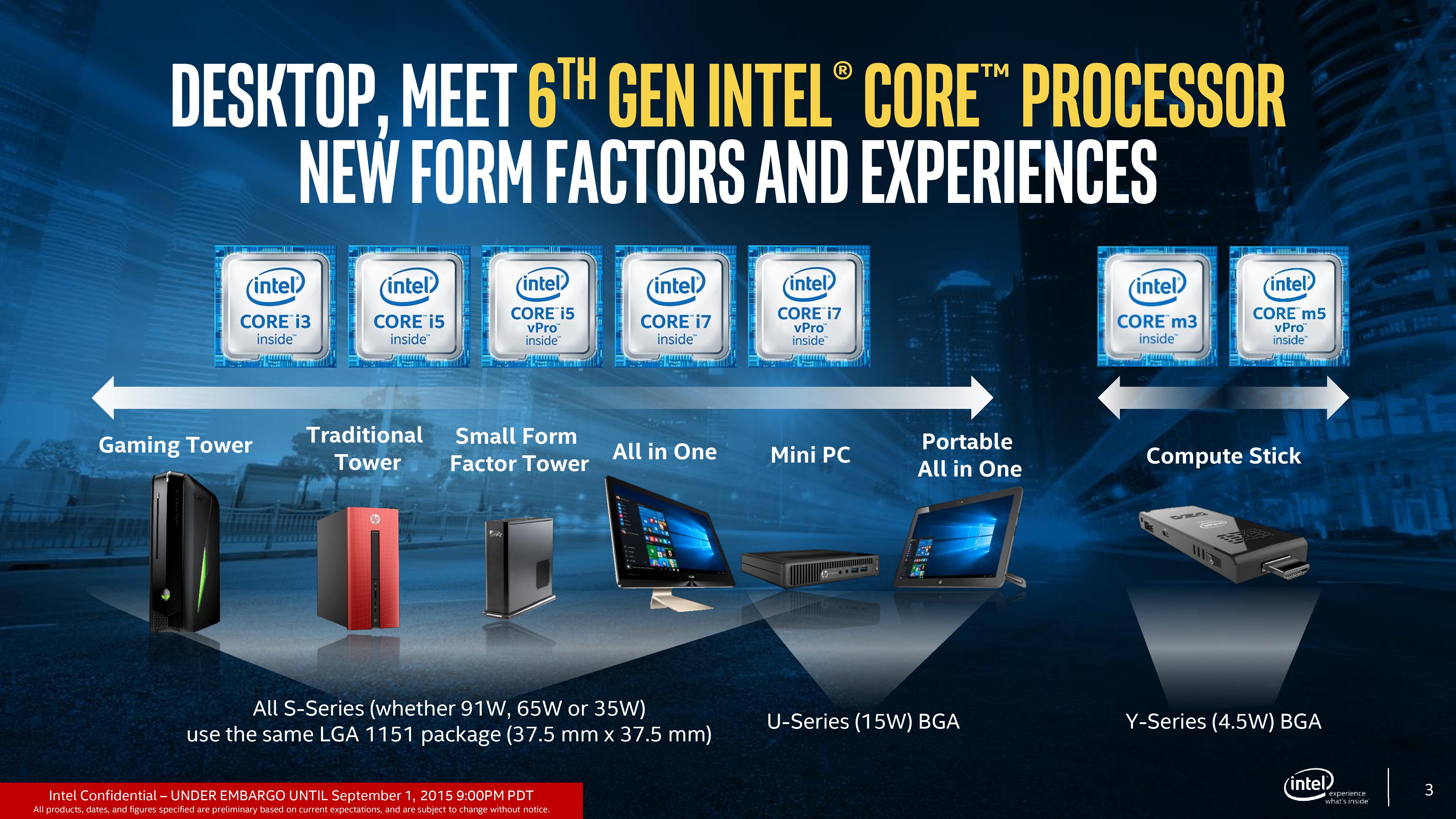
On the Skylake-S side of the equation, the processors come in two segments. Here is the list of the low powered processors that have the ‘T’ in the name, or unofficially known as ‘Skylake-T’. These are all 35W, some with vPro, but covering the i3/i5/i7 lines sufficiently.

The non-T and non-K desktop processors come in at 65W, and there are no real surprises here in the product lines as they migrate well enough from previous generation designations. All the Skylake-S i3/i5/i7 processors have HD 530 graphics.
Beyond Skylake and to Kaby Lake
Post Skylake, Intel is breaking from the tick-model to tick-tock-tock, posting a third generation on 14nm called Kaby Lake (pronounced Kah-bee, as far as we were told).
This stems from the issues of moving to smaller process nodes. At 14nm, this equates to only 90 silicon atoms, meaning ever more intensive manufacturing is required which drives up cost and reduces yield. Due to the issues Intel had at 14nm using their second generation FinFET method and more advanced double patterning, initial costs were high and yields were lower than expected for the timeframe, pushing Broadwell to a later-than-expected timeline. Skylake was kept to the regular timeline, resulting in a brief outing for Broadwell (on the desktop especially). But we suspect that similar reasoning is behind a delay from 14nm to 10nm –more esoteric ways under conventional methodology are required to keep driving the node down, and with that comes extra challenges that delay both time to market and yield numbers before tweaking the design.
We’ve mentioned in the past that the development of extreme-ultra-violet (EUV) technology is one element that could assist this drive down, however Intel is not expected to implement this for 10nm but rather for 7nm, which is still several years down the road. To that end, tick-tock is not dead, but merely stretching out.


173 Comments
View All Comments
jay401 - Wednesday, September 2, 2015 - link
Sounds about right, actually.asmian - Thursday, September 3, 2015 - link
Yeah, I'd like to see MUCH more comment and examination on the reasons for this. It may be being spun as something to prevent malware from attacking other legitimate processes, but it's equally a box of delights for malware of any kind if it can insert itself into a protected zone and have all its code and data safe from any debugging or monitoring. And when I say malware of any kind, NSA back door is indeed what screams loudest to me. With MS preventing users from refusing individual updates to Windows 10, that's a mass surveillance perfect storm just waiting to happen down the line unless there is intense scrutiny of any use of this.The risk in this single feature could be the deciding factor for me not to move beyond Haswell-E with Intel.
hojnikb - Wednesday, September 2, 2015 - link
Is it possible to overclock non-k parts, given that blck is uncoupled from the rest of the system ?MrSpadge - Wednesday, September 2, 2015 - link
I'd want to know that as well. And is there still "multicore optimization", i.e. max turbo freqeuncy for all cores? With an increased power budget this would make the 6700 fly.. while staying in an energy efficient regime, in contrast to full-throttle OC of the 6700K.extide - Wednesday, September 2, 2015 - link
I am thinking ... yes at least on Z170 ... but the other chipsets, I dont know. Could be really fun :)hojnikb - Thursday, September 3, 2015 - link
Could someone test this ?Even if its limited to Z chipsets, its still great. I'm sure if that is actually possible, some mobo maker will come up with cheapish Z boards (like asrock).
extide - Saturday, September 5, 2015 - link
I'm sure plenty of people will test it, once the parts are actually in peoples hands.cactusdog - Wednesday, September 2, 2015 - link
Will the Intel muthaphuckers make a CPU faster than the 6700K for Skylake?just4U - Wednesday, September 2, 2015 - link
Of course they will.. just as you go out to buy your 6700K in a year or two they will release a 6790K /w better thermal dynamics.. (Let's not hold our breath on 6 Core puppies.. Intel doesn't seem interested as long as they have no competition)prisonerX - Saturday, September 5, 2015 - link
"Better thermal dynamics"? Is that an euphemism for Intel getting better at throttling your CPU?Actually it's not a euphemism, it's exactly what it means. Certainly worth another $300!