The Intel 6th Gen Skylake Review: Core i7-6700K and i5-6600K Tested
by Ian Cutress on August 5, 2015 8:00 AM ESTThe Skylake CPU Architecture
As with any new Intel architecture, the devil is in the details. Previously at AnandTech we have been able to provide deep dives into what exactly is going on in the belly of the beast, although the launch of Skylake has posed a fair share of problems.
Nominally we rely on a certain amount of openness from the processor/SoC manufacturer in providing low level details that we can verify and/or explain. In the past, this information has typically been provided in advance of the launch by way of several meetings/consultations with discussions talking to the engineers. There are some things we can probe, but others are like a black box. The black box nature of some elements, such as Qualcomm’s Adreno graphics, means that it will remain a mystery until Pandora’s box is opened.
In the lead up to the launch of Intel’s Skylake platform, architecture details have been both thin on the ground and thin in the air, even when it comes down to fundamental details about the EU counts of the integrated graphics, or explanations regarding the change in processor naming scheme. In almost all circumstances, we’ve been told to wait until Intel’s Developer Forum in mid-August for the main reason that the launch today is not the full stack Skylake launch, which will take place later in the quarter. Both Ryan and I will be at IDF taking fastidious notes and asking questions for everyone, but at this point in time a good portion of our analysis comes from information provided by sources other than Intel, and while we trust it, we can't fully verify it as we normally would.
As a result, the details on the following few pages have been formed through investigation, discussion and collaboration outside the normal channels, and may be updated as more information is discovered or confirmed. Some of this information is mirrored in our other coverage in order to offer a complete picture in each article as well. After IDF we plan to put together a more detailed architecture piece as a fundamental block in analyzing our end results.
The CPU
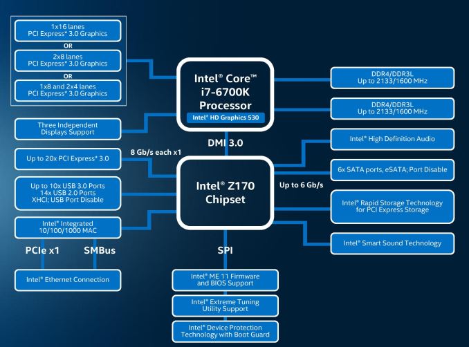
As bad as it sounds, the best image of the underlying processor architecture is the block diagram:
From a CPU connectivity standpoint, we discussed the DDR3L/DDR4 dual memory controller design on the previous page so we won’t go over it again here. On the PCI-Express Graphics allocation side, the Skylake processors will have sixteen PCIe 3.0 lanes to use for directly attached devices to the processor, similar to Intel's previous generation processors. These can be split into a single PCIe 3.0 x16, x8/x8 or x8/x4/x4 with basic motherboard design. (Note that this is different to early reports of Skylake having 20 PCIe 3.0 lanes for GPUs. It does not.)
With this, SLI will work up to x8/x8. If a motherboard supports x8/x4/x4 and a PCIe card is placed into that bottom slot, SLI will not work because only one GPU will have eight lanes. NVIDIA requires a minimum of PCIe x8 in order to enable SLI. Crossfire has no such limitation, which makes the possible configurations interesting. Below we discuss that the chipset has 20 (!) PCIe 3.0 lanes to use in five sets of four lanes, and these could be used for graphics cards as well. That means a motherboard can support x8/x8 from the CPU and PCIe 3.0 x4 from the chipset and end up with either dual-SLI or tri-CFX enabled when all the slots are populated.
DMI 3.0
The processor is connected to the chipset by the four-lane DMI 3.0 interface. The DMI 3.0 protocol is an upgrade over the previous generation which used DMI 2.0 – this upgrade boosts the speed from 5.0 GT/s (2GB/sec) to 8.0 GT/s (~3.93GB/sec), essentially upgrading DMI from PCIe 2 to PCIe 3, but requires the motherboard traces between the CPU and chipset to be shorter (7 inches rather than 8 inches) in order to maintain signal speed and integrity. This also allows one of the biggest upgrades to the system, chipset connectivity, as shown below in the HSIO section.
CPU Power Arrangements
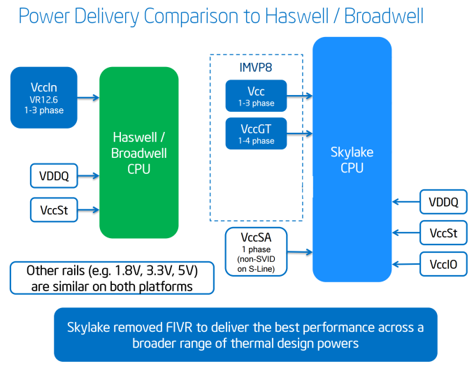
Moving on to power arrangements, with Skylake the situation changes as compared to Haswell. Prior to Haswell, voltage regulation was performed by the motherboard and the right voltages were then put into the processor. This was deemed inefficient for power consumption, and for the Haswell/Broadwell processors Intel decided to create a fully integrated voltage regulator (FIVR) in order to reduce motherboard cost and reduce power consumption. This had an unintended side-effect – while it was more efficient (good for mobile platforms), it also acted as a source of heat generation inside the CPU with high frequencies. As a result, overclocking was limited by temperatures and the quality of the FIVR led to a large variation in results. For Skylake on the desktop, the voltage regulation is moved back into the hands of the motherboard manufacturers. This should allow for cooler processors depending on how the silicon works, but it will result in slightly more expensive motherboards.
A slight indication of this will be that some motherboards will go back to having a large amount of multiplexed phases on the motherboard, and it will allow some manufacturers to use this as a differentiating point, although the usefulness of such a design is sometimes questionable.


477 Comments
View All Comments
mkozakewich - Thursday, August 6, 2015 - link
It's unlikely you'll be seeing doubles and doubles anymore. If you look at what's been going on for the past several years, we're moving to more efficient processes instead of improving performance. I'm sure Intel's end goal is to make powerful CPUs for devices that fit into people's pockets. At that point you might see more start going into raw performance.edlee - Wednesday, August 5, 2015 - link
i am not sure why conclusion to the review makes it seem i7-2600k users should upgrade to this.If you are a gamer, there is no 25% improvement in average or minimum frame rate, its 3-6% at best.
Is this the future of intel's tock strategy, to give very little improvement to gamers?
VeauX - Wednesday, August 5, 2015 - link
On the gaming side, you'll never see a speed bump if you are not CPU Limited. Once you have a decent CPU, just put your money in GPU, period.Nagorak - Wednesday, August 5, 2015 - link
CPU is almost irrelevant for games at this point. As games start to take advantage of more cores, older processors are utilized more efficiently, further negating the need to upgrade. DX12 may improve this further.I sort of wonder if Intel isn't on a path to some trouble here. There's basically no point for anyone to upgrade their CPU anymore, not even gamers. Other than a few specialized applications the increase in performance just doesn't really matter, if it exists at all.
AndrewJacksonZA - Thursday, August 6, 2015 - link
I also sometimes think that, but then I remember that we developers *WILL* find a way to make use of more computing power.Having said that, I still can't quite justify me upgrading from my E6750 and 6670 @ 1240 x 1024. I slapped in an SSD in February last year and it was like I got a brand new machine.
Chrome and Edge on Win10 lag a teeny tiny bit though, maybe I can use that as my justification... Perhaps a 5960X or a 5930K though - more cores FTW? Or perhaps a 6700K and get it to 5GHz for the rights to claim some "5GHz Daily Driver" epeen... ;-)
Zoomer - Friday, August 14, 2015 - link
Exactly, I reached the opposite conclusion as Ian. There is no point in upgrading even from SB. If you do, stick to DDR3. Only GTA5 benefits from DDR4.It's interesting to see if regular DDR3 sticks can run on Skylake, perhaps by bumping the Vsa, voltages. Not clear if Ian's overclocking tests were with the IGP disabled - would be interesting to see if disabling the IGP / reducing Fgt, Vgt helps overclocking any.
StevoLincolnite - Wednesday, August 5, 2015 - link
I'm still happily sitting with my Sandy-Bridge-E. Still handles everything you could throw at it just fine... And still gives Intel's $1,000 chips a run for their money whilst sitting at 5Ghz.mapesdhs - Wednesday, August 12, 2015 - link
Yup, that's why my most recent gaming build was a R4E & 3930K, cost less than a new HW build, much quicker overall. My existing SB gaming PC is 5GHz aswell (every 2700K I've tried handles 5.0 just fine).leexgx - Monday, August 10, 2015 - link
hmm maybe i can upgrade from my i7-920 now (really any of the newer intel cpus are faster then it)sheeple - Thursday, October 15, 2015 - link
DON'T BE STUPID SHEEPLE!!! NEW DOES NOT ALWAYS = BETTER!