Analyzing Intel-Micron 3D XPoint: The Next Generation Non-Volatile Memory
by Kristian Vättö, Ian Cutress & Ryan Smith on July 31, 2015 11:00 AM ESTEstimating 3D XPoint Die Size
By now most of you probably know that I'm a sucker for die sizes and since this is information that the DRAM and NAND vendors are unwilling to share, I've gone as far as developing my own method for estimating the die size (well, it's really just primary school geometry, so I can't take too much credit for it). Die size is the key factor in determining cost efficiency because it directly relates to the number of gigabytes each wafer yields and thus it's a vital metric for comparing different technologies and process nodes.
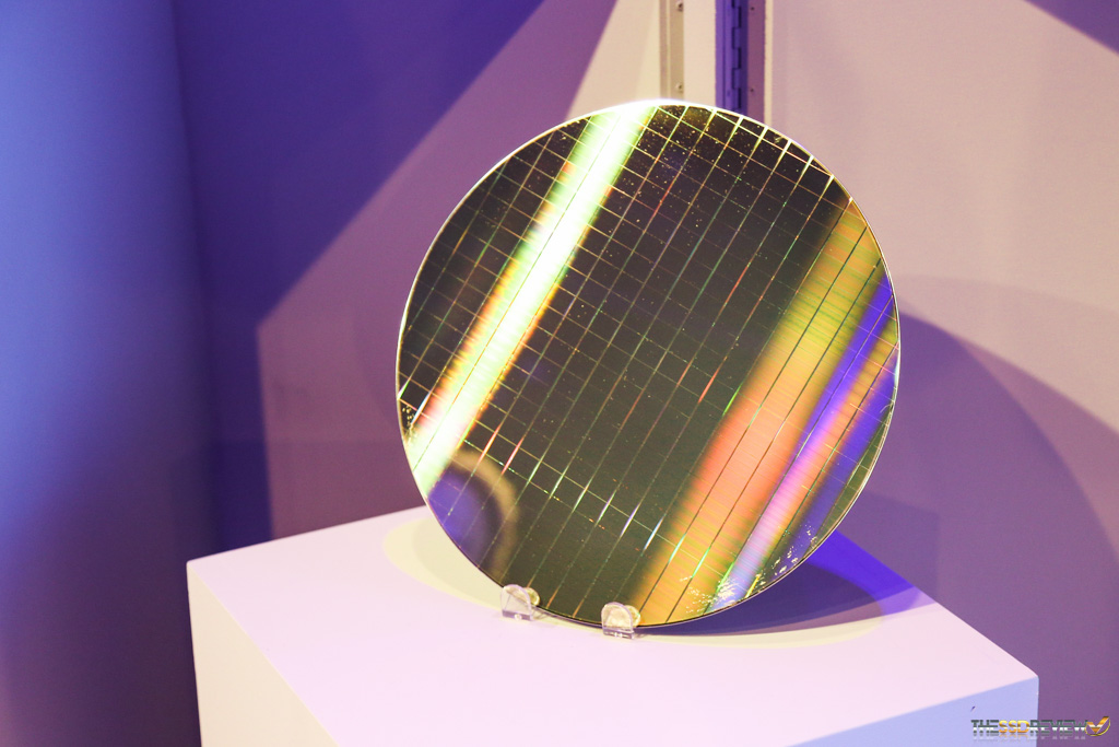
I'm borrowing the above picture from The SSD Review because to be honest my wafer photos (and photos in general) are quite horrible and wafers are far from being the easiest object given all the reflections. Sean is a professional photographer, so he managed to grab this clear and beautiful photo of the production 3D XPoint wafer Intel and Micron had on display, making it easy to estimate the die size.
I calculated 18 dies horizontally and 22 vertically, which yields 227mm^2 with a normal 300mm wafer. When taking die cuts (i.e. the space between dies) into account, we should be looking at 210-220mm^2. Array efficiency is about 90%, which is much higher than planar NAND because most of the peripheral circuitry lies underneath the memory array.
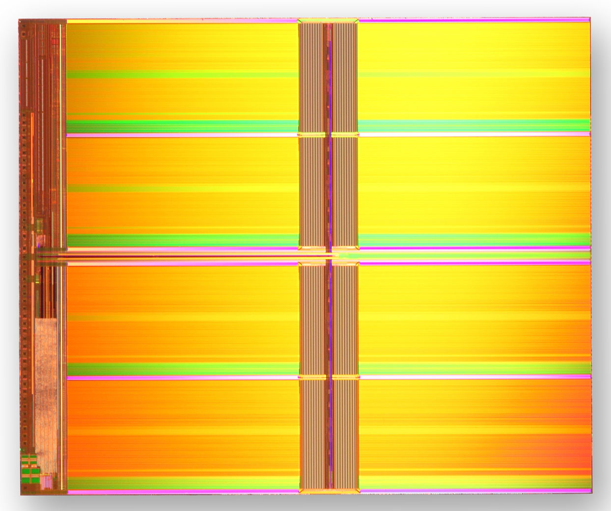
IMFT 20nm 128Gbit MLC NAND die
For comparison, Intel-Micron's 20nm 128Gbit MLC NAND die measures 202mm^2 and has array efficiency of ~75%. From that we can calculate that the 128Gbit memory array in 3D XPoint takes about 190mm^2, while a similar capacity planar NAND array measures ~150mm^2 (since the 128Gbit 3D XPoint die consists of two layers and 128Gbit MLC NAND die stores two bits per cell, the number of layers and bits stored per cell cancel out). It seems like NAND is denser (about 20-25%) from a memory array perspective given a fixed feature size (i.e. lithography), but at this point it's hard to say whether this is due to the cell design itself or something else. Connecting layers of wordlines and bitlines to the intermetal layers likely takes some extra area compared to a 2D process (at least this is the case with 3D NAND), which might partially explain the lower density compared to NAND.
However we will have to wait for some SEM photos to really see what's happening inside the 3D XPoint array and how it compares to NAND in cell size and overall density efficiency. Of course, there is a lot more in total manufacturing cost than just the cell and die size, but I'll leave the full analysis to those with the proper equipment and deeper knowledge of semiconductor manufacturing processes.
What Happens to 3D NAND
The above analysis already gives a hint that 3D XPoint isn't about to replace 3D NAND, at least not in the foreseeable future. That's also what Intel and Micron clearly stated when asked about 3D XPoint's impact on 3D NAND because it's really a new class of memory that fills a niche that DRAM and NAND cannot. The companies are still looking forward to rolling out 3D NAND next year and have a strong roadmap of future 3D NAND generations.
As I mentioned earlier, the way 3D XPoint array is built is quite different from 3D NAND and my understanding is that it's less economical, which is one of the reasons why the first generation product is a two-layer design at 20nm rather than dozens of layers at a larger lithography with single patterning like 3D NAND is. Unless there's a way to build 3D XPoint arrays more like 3D NAND (i.e. pattern and etch multiple layers at the same time), I don't see 3D XPoint becoming cost competitive with 3D NAND anytime soon, but then again it's not aimed to be a NAND successor in short-term.
What happens in ten year's time is a different question, though. 3D NAND does have some inherent scaling obstacles with vanishing string current likely being the biggest and most well known at this point. Basically, the channel in each 3D NAND "cell tower" (i.e. a stack of layers, currently 32 for Samsung and Intel-Micron) is a single string that the electrons have to flow through to reach every individual cell in the string. The problem is that as the length of the string increases (i.e. more layers are added), it becomes harder to reach the top cells because the cells on the way cause disturbance, reducing the overall string current (hence the name "vanishing string current"). For those who are interested in a more detailed explanation of this issue along with some experimental data, I suggest you head over to 3D Incites and read Andrew Walker's post on the topic.
Since most vendors haven't even started 3D NAND mass production, it's not like the technology is going to hit a wall anytime soon and e.g. Toshiba-SanDisk's 15nm NAND has strings consisting of 128 cells, but like any semiconductor technology 3D NAND will reach a scaling limit at some point. Whether that is in five, ten or twenty years is unknown, but having a mature and scalable technology like what 3D XPoint should be at that point is important.


80 Comments
View All Comments
Kristian Vättö - Monday, August 3, 2015 - link
That's a good point and admittedly something I didn't think about. I would assume 3D XPoint is more robust than NAND given the higher performance and endurance, but Intel/Micron declined to talk about any failure mechanisms, so at this point it's hard to say how robust the technology is.Nilth - Sunday, August 2, 2015 - link
Well, I really hope it won't take 10 years to see this technology at the consumer level.dotpex - Monday, August 3, 2015 - link
From Micron site https://www.micron.com/about/innovations/3d-xpoint..."Memory cells are accessed and written or read by varying the amount of voltage sent to each selector. This eliminates the need for transistors, increasing capacity and reducing cost."
...but 3d xpoint will be expensive, more like $10 per gigabyte.
Adam Bise - Friday, August 7, 2015 - link
"First and foremost, Intel and Micron are making it clear that they are not positioning 3D XPoint as a replacement technology for either NAND or DRAM"I wonder if this is because they would rather create a new market than replace an existing one.
hans_ober - Saturday, August 8, 2015 - link
@Ian. PhD Chem was useful! :)Ian Cutress - Monday, September 28, 2015 - link
Yiss :)duartix - Monday, August 10, 2015 - link
I see two immediate consumer usages:a) Instant Go To / Wake From deep hibernation
b) Scratch disks
MRFS - Monday, August 24, 2015 - link
With proper UEFI/BIOS support, one feature we proposed in a Provisional Patent Application was a "Format RAM" option prior to running Windows Setup. This would format RAM as an NTFS C: partition into which Windows software would be freshly installed. For comparison purposes, imagine a ramdisk in the upper 32-to-64GB of a large 1-to-2 TB DRAM subsystem, in a manner similar to how SuperSpeed's RamDisk Plus allocates RAM addresses. Then, imagine that all 2 TB consist of Non-Volatile DIMMs. I can see this one feature enabling very rapid RESTARTS, even cold RESTARTS after a full power-down (for maintenance). If the UEFI/BIOS is told that the OS is already memory-resident, this one change radically improves the speed with which a routine STARTUP occurs i.e. currently a STARTUP must load all OS software from a storage subsystem into RAM. If that OS software is already loaded into RAM, that "loading" is mostly eliminated under these new assumptions. Moreover, mounting Optane on the 2.5" form factor should free designers to consider more aggressive overclocking of the data cables connecting motherboards to those 2.5" drives: just work backwards from PCIe 4.0's 16GHz clock and 128b/130b jumbo frame. It's possible that Optane will be fast enough to justify data cables that also oscillate at 16GHz, increasing to 32GHz with predictable success. Assuming x4 NVMe lanes at PCIe 4.0, then 4 lanes @ (16G / 8.125) ~= 4 lanes @ 2GB/s ~= 8 GB/s raw bandwidth per 2.5" device. Modern G.Skill DDR4 easily exceeds 25GB/s raw bandwidth. Thus, Optane should allow "overclocked" data cables to achieve blistering NVMe storage performance with JBOD devices, and even higher performance with RAID-0 arrays.FutureCTO - Tuesday, November 15, 2016 - link
I don't know, is it possible to have an educated guess on this? Back in the PS2 days, before the PS3, i was @0zyx on forum or few, talking about NASA RAM, magnet donuts on a metal grid of wires, insisting why don't we do this with memory today? The electricity crosses and creates a charge or reads the charge. This is the RAM of the first space computer. ~ I was made confident by believing this is what AMD "Mirror Bit" Memory was working towards before it flat out evaporated from the internet? Same happened to 48Bit Intel "Iranium" processors with 16cores. Still look in books from time to time, hoping an old edition of hardware lists with intel spy cpu, will confirm the internet is a BlackHole. Not to go Ellery Hale, with being one of those to store curious science bits no one is using, and everyone should be clamoring to own some day. ~ I check the metal recycling at the city dump for computer servers and extra high grade tower cases for my own builds, at least a parts from the towers anyways. ~ Twitter @0zyx ~ either way this is the memory design from the first NASA space capsule to carry people into space, except larger than 1 kilobyte. It may have been 512Bytes back then, not sure what sort of grid that is?FutureCTO - Tuesday, November 15, 2016 - link
educated guess on price? ~ To me it is simpler to make, and faster to verify trace integrity.