Analyzing Intel-Micron 3D XPoint: The Next Generation Non-Volatile Memory
by Kristian Vättö, Ian Cutress & Ryan Smith on July 31, 2015 11:00 AM ESTEstimating 3D XPoint Die Size
By now most of you probably know that I'm a sucker for die sizes and since this is information that the DRAM and NAND vendors are unwilling to share, I've gone as far as developing my own method for estimating the die size (well, it's really just primary school geometry, so I can't take too much credit for it). Die size is the key factor in determining cost efficiency because it directly relates to the number of gigabytes each wafer yields and thus it's a vital metric for comparing different technologies and process nodes.
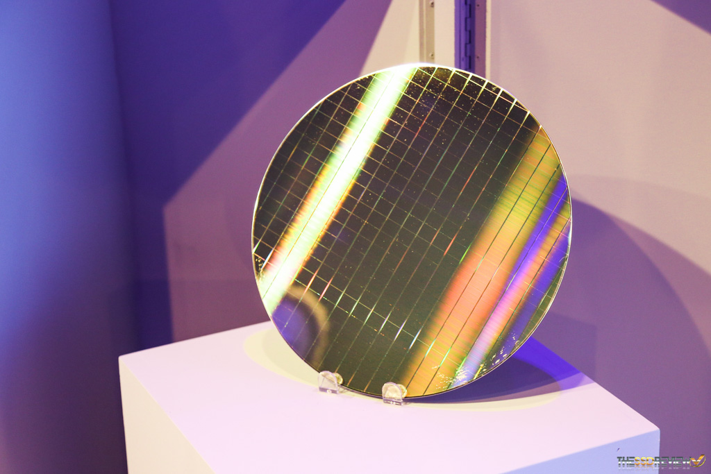
I'm borrowing the above picture from The SSD Review because to be honest my wafer photos (and photos in general) are quite horrible and wafers are far from being the easiest object given all the reflections. Sean is a professional photographer, so he managed to grab this clear and beautiful photo of the production 3D XPoint wafer Intel and Micron had on display, making it easy to estimate the die size.
I calculated 18 dies horizontally and 22 vertically, which yields 227mm^2 with a normal 300mm wafer. When taking die cuts (i.e. the space between dies) into account, we should be looking at 210-220mm^2. Array efficiency is about 90%, which is much higher than planar NAND because most of the peripheral circuitry lies underneath the memory array.
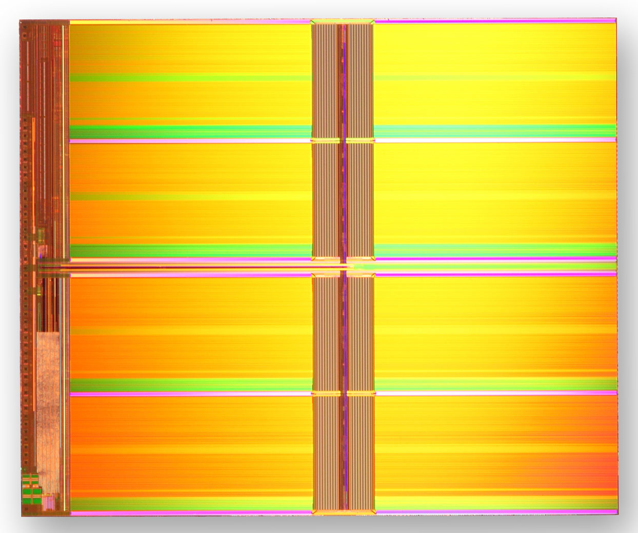
IMFT 20nm 128Gbit MLC NAND die
For comparison, Intel-Micron's 20nm 128Gbit MLC NAND die measures 202mm^2 and has array efficiency of ~75%. From that we can calculate that the 128Gbit memory array in 3D XPoint takes about 190mm^2, while a similar capacity planar NAND array measures ~150mm^2 (since the 128Gbit 3D XPoint die consists of two layers and 128Gbit MLC NAND die stores two bits per cell, the number of layers and bits stored per cell cancel out). It seems like NAND is denser (about 20-25%) from a memory array perspective given a fixed feature size (i.e. lithography), but at this point it's hard to say whether this is due to the cell design itself or something else. Connecting layers of wordlines and bitlines to the intermetal layers likely takes some extra area compared to a 2D process (at least this is the case with 3D NAND), which might partially explain the lower density compared to NAND.
However we will have to wait for some SEM photos to really see what's happening inside the 3D XPoint array and how it compares to NAND in cell size and overall density efficiency. Of course, there is a lot more in total manufacturing cost than just the cell and die size, but I'll leave the full analysis to those with the proper equipment and deeper knowledge of semiconductor manufacturing processes.
What Happens to 3D NAND
The above analysis already gives a hint that 3D XPoint isn't about to replace 3D NAND, at least not in the foreseeable future. That's also what Intel and Micron clearly stated when asked about 3D XPoint's impact on 3D NAND because it's really a new class of memory that fills a niche that DRAM and NAND cannot. The companies are still looking forward to rolling out 3D NAND next year and have a strong roadmap of future 3D NAND generations.
As I mentioned earlier, the way 3D XPoint array is built is quite different from 3D NAND and my understanding is that it's less economical, which is one of the reasons why the first generation product is a two-layer design at 20nm rather than dozens of layers at a larger lithography with single patterning like 3D NAND is. Unless there's a way to build 3D XPoint arrays more like 3D NAND (i.e. pattern and etch multiple layers at the same time), I don't see 3D XPoint becoming cost competitive with 3D NAND anytime soon, but then again it's not aimed to be a NAND successor in short-term.
What happens in ten year's time is a different question, though. 3D NAND does have some inherent scaling obstacles with vanishing string current likely being the biggest and most well known at this point. Basically, the channel in each 3D NAND "cell tower" (i.e. a stack of layers, currently 32 for Samsung and Intel-Micron) is a single string that the electrons have to flow through to reach every individual cell in the string. The problem is that as the length of the string increases (i.e. more layers are added), it becomes harder to reach the top cells because the cells on the way cause disturbance, reducing the overall string current (hence the name "vanishing string current"). For those who are interested in a more detailed explanation of this issue along with some experimental data, I suggest you head over to 3D Incites and read Andrew Walker's post on the topic.
Since most vendors haven't even started 3D NAND mass production, it's not like the technology is going to hit a wall anytime soon and e.g. Toshiba-SanDisk's 15nm NAND has strings consisting of 128 cells, but like any semiconductor technology 3D NAND will reach a scaling limit at some point. Whether that is in five, ten or twenty years is unknown, but having a mature and scalable technology like what 3D XPoint should be at that point is important.


80 Comments
View All Comments
wishgranter - Saturday, August 1, 2015 - link
As always, waited for Anand to tear it to the point and explain it as they did it,this is stuff that differ you from other "news" sites... So let see what they bring to market...
azazel1024 - Saturday, August 1, 2015 - link
Great, so now I need to get a boot drive again.DRAM, XPOINT boot drive, SSD application drive and HDD bulk storage. Maybe we can usher in holographic storage and have another tier! I mostly kid, but man getting excessive. It would be cool if this was added in through new/advanced memory controllers and utilize the DRAM slots. If the price is at least reasonably less than DRAM (by at least a factor of 2), I can see uses. A legit OS drive space. Useful for higher end tablets and stuff with embedded high speed storage. A serious swap disk, etc.
16GB of RAM with 32-64GB of XPOINT and then the SSD/HDD storage systems would probably make a pretty wicked system. Use the XPOINT to do things like load large parts of games/applications in a super fast swap disk pre-loading as much as possible and then quickly import the parts in to RAM that are needed instead of slower imports from SSD/HDD to RAM.
A little disappointed that this doesn't sound like it'll be remotely economical to compete with NAND anytime soon. I had my hopes up with the density claims and what not that we might have a NAND replacement at HDD price per GB in a couple of years.
userDavid - Saturday, August 1, 2015 - link
"SPoint" is my guess for pronunciation. If the marketing idiots can't spell out "3D CrossPoint", I don't think we're obliged to pronounce it that way.jay401 - Saturday, August 1, 2015 - link
"A quick look at NewEgg puts DRAM pricing at approximately $5-6 per gigabyte, whereas the high-end enterprise SSDs are in the range of $2-3. While client SSDs can be had for as low as $0.35, they aren't really a fair comparison because at least initially 3D XPoint will be aimed for enterprise applications. My educated guess is that the first 3D XPoint based products will be priced at about $4 per gigabyte, possibly even slightly lower depending on how DRAM and NAND pricess fall within a year."Oh, okay, see you in five years or so, when this technology becomes relevant to the consumer. @___@
Crazy1 - Saturday, August 1, 2015 - link
I hate that Intel and Micron didn't talk about potential uses for this new technology. Letting my imagination run wild, I'm thinking small, battery powered embedded solutions is a good starting point. Basically IoT devices, from infrastructure sensors on up to smart watches. There are not many market standards in place in this category of computing devices and energy efficiency is more important than high performance. This XPoint tech could replace both NAND and DRAM in these devices, presumably increasing energy efficiency. It also provides small, adaptable platforms for developers to start programming for applications with no RAM.I don't see XPoint replacing DRAM and NAND in smartphones and tablets any time soon. I assume it will take a while before OSes and apps can adapt to a no RAM environment. It will take a few SoC generations for this tech to have hardware support as well (unless they were already in-the-know). Smaller issues include degraded performance in RAM heavy applications (i.e. graphics processing) and increased hardware costs. The GPU might need its own RAM buffer (might I suggest HBM), further increasing implementation costs. Also, encrypted storage gets a little costly, from an energy perspective, when that storage bandwidth is very fast. Ideally, there will be a hardware encryption accelerator in the mix (and the OS will implement it (looking at you Android)).
However, there are a lot of potential benefits to replacing RAM and NAND completely with XPoint from a smart phone. The device could turn on and off almost instantly. Power management would not need to deal with the energy costs of shuffling around large amounts of data to enter and exit a sleep state. OSes and apps would be smaller and more efficient due to significantly reduced memory management concerns (some minimal wear leveling and ECC).
The first implementation of XPoint in smartphones/tablets will probably be as an added cache to accelerate the NAND and act as a swap partition. The NAND eMMC in most smart phones is more competitive with a modern HDD than a SSD when it comes to transfer speeds, so the NAND could definitely use a boost.
The day XPoint replaces NAND SSD's in the consumer space will be glorious. If speculation on price is correct, it may be a while before even the average enthusiast can rationalize the expense. However, I did see an Intel video that described DRAM as expensive and both XPoint and NAND as inexpensive. So, it would stand to reason that XPoint would be closer to the price of NAND than DRAM once initial market shock has subsided a bit and production has ramped up. However, Intel is rarely known to offer inexpensive products compared to its competition, so the real hope is that Micron pushes this technology at a price and quantity that stimulates quick market adoption.
Brane2 - Saturday, August 1, 2015 - link
How the heck can you "analyze" something that you know practically nothing about ?All you have is a bit of marketing fluff and you are building virtual castles out of that....
Laststop311 - Saturday, August 1, 2015 - link
maybe bias is affecting me but it seems the quality of articles has gone down since this site was sold and anand left.Kristian Vättö - Monday, August 3, 2015 - link
Could you elaborate? I think this article in particular is far more in-depth than any of the other articles I've read on the topic and it really goes into great detail about the physics side as well.speculatrix - Sunday, August 2, 2015 - link
typo "either slower, non-volitile memory" - volAtileVetri33 - Sunday, August 2, 2015 - link
There is NO mention of the error rate in 3D Xpoint compare to Enterprise NAND!?. This may make a big difference in Enterprise SSD Controller architecture & implementation like whether LDPC, BCH or a very simple Error Correction algorithm is good enough!?. The power is an another big factor especially in Write, One of the main limiting factor in enterprise SSD write performance is the power budget.