AMD Launches Carrizo: The Laptop Leap of Efficiency and Architecture Updates
by Ian Cutress on June 2, 2015 9:00 PM ESTUnified Video Decoder and Playback Pathways
A typical consumer user experience revolves a lot around video, and AMD identified for Carrizo a big potential to decrease power consumption and increase performance in a couple of different ways. First up is adjusting the path by which data is moved around the system, particularly as not a lot of video matches up with the native resolution of the screen or is scaled 1:1.
When a video exhibits a form of scaling, either it is made full screen and scaled up or it is a higher resolution video that scales down, that scaling is typically performed by the GPU. The data leaves the decoder (either hardware or software), enters system memory, moves into the graphics memory, is processed by the GPU, moves back out to memory, and then is transferred to the display. This requires multiple read/write commands to memory, requires the GPU to be active but underutilized, and this happens for every frame. AMD’s solution to this is to provide some simple scaling IP in the display engine itself, allowing for scaled video to go from the decoder to the display engine, leaving the GPU in a low power state.
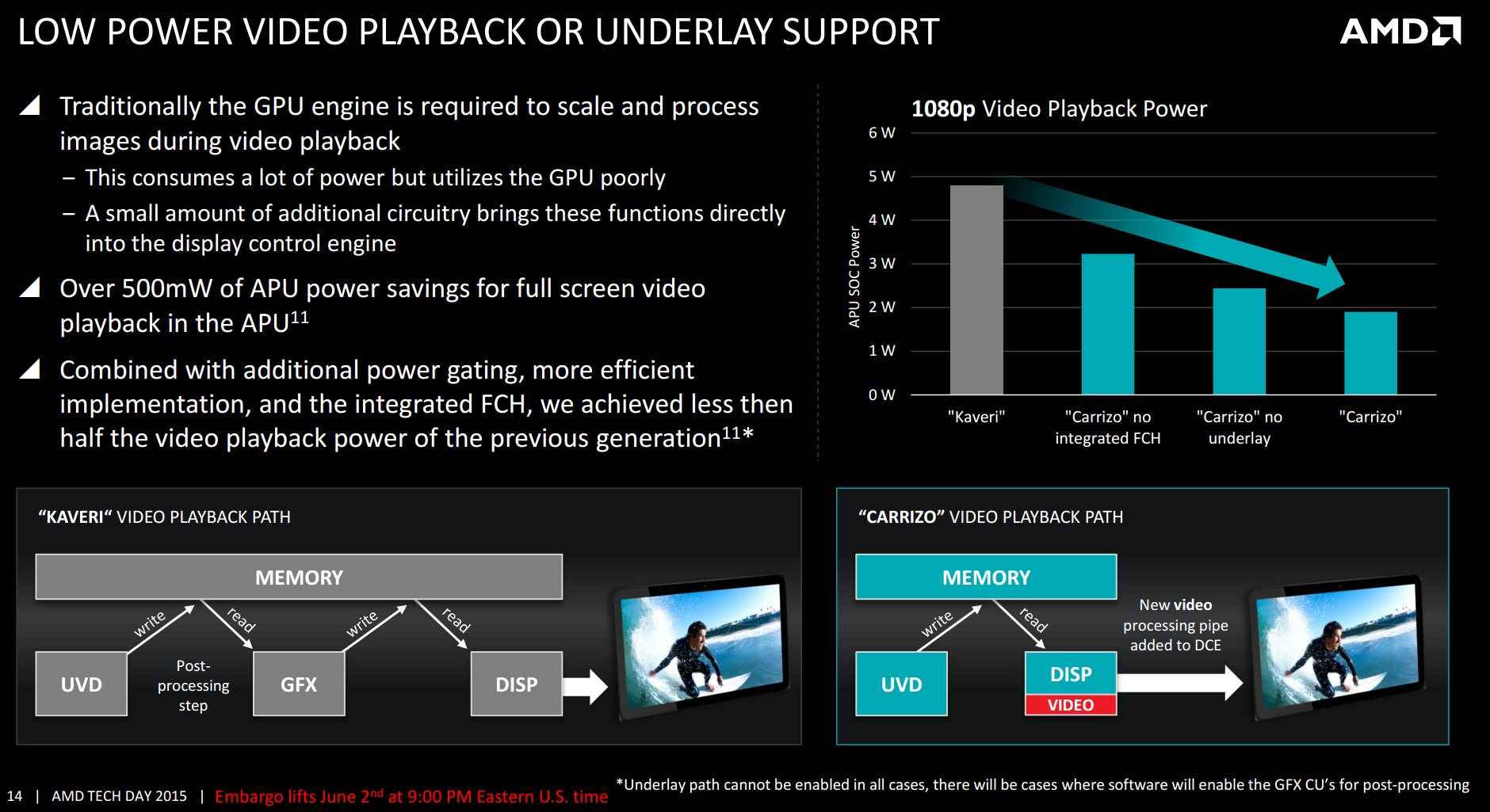
The video playback paths at the bottom of this side show the explanation graphically, and AMD is quoting a 4.8W down to 1.9W movement in power consumption for these tasks. Note that the 4.8W value is for Kaveri, so there are other enhancements in there is as well, but the overall picture is a positive one and AMD quotes a 500mW of APU power savings.
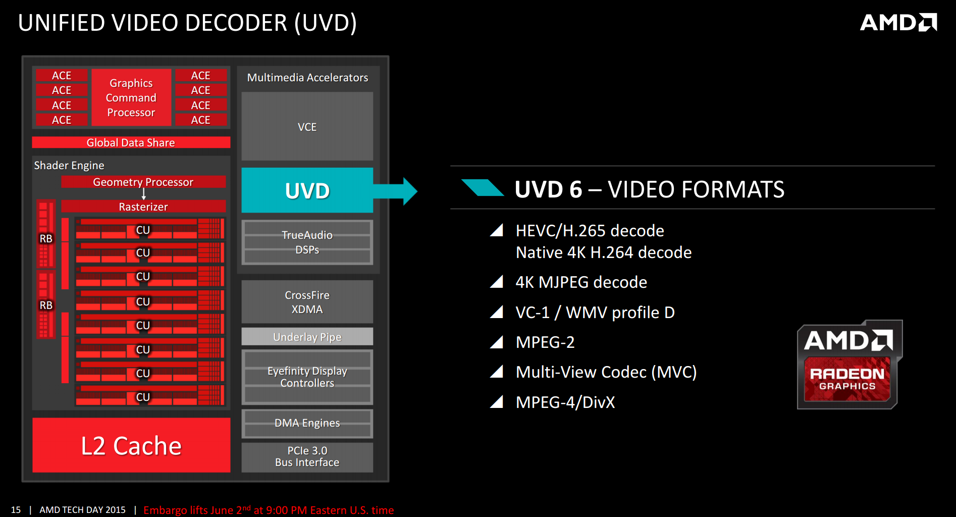
The Unified Video Decoder (UVD) has been built to support the above codecs, with HEVC decode on die as well as native 4K H.264 decode as well. I’ll come back to the 4K element in a second, but what is perhaps missing from this list is VP9, the codec used by Google for YouTube. YouTube is still the number one source for video content on the web, and as Google is transitioning more to VP9, as well as AMD’s competition advertising it as a perk on their latest hardware, it was perhaps confusing for AMD to miss it out. I did ask on this, and was told that they picked HEVC over VP9 as they believe it will be the more important codec going forward, particularly when you consider that the majority of the popular streaming services (NetFlix, Hulu, Amazon) will be using HEVC for their high definition titles.
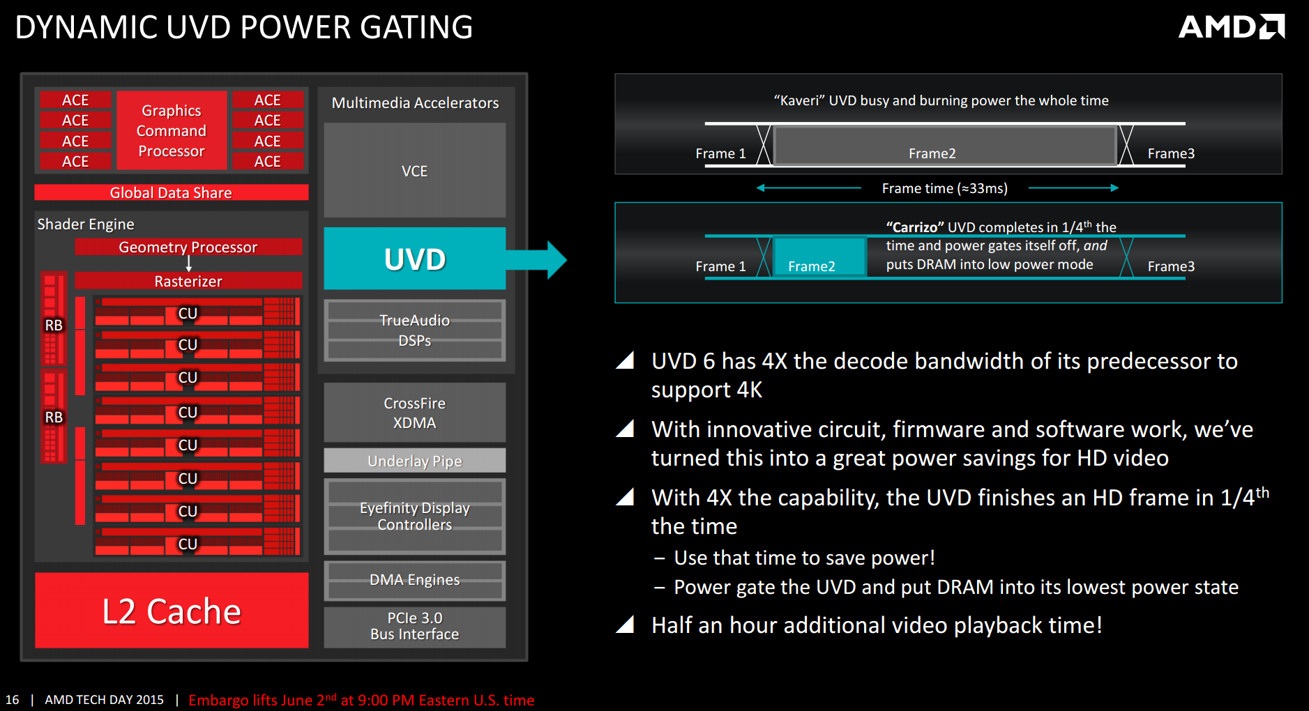
Back onto the 4K equation, and this is possible because AMD has increased the decode bandwidth of the UVD from 1080p to 4K. This affords two opportunities – 4K video on the fly, or 1080p video decoded in a quarter of the time, allowing the race to sleep for both the UVD and DRAM. Despite a 75% reduction in work, as the UVD does not use that much power, it results in only 30 minutes of extra video playback time, but it is welcome and contributes to that often marketed ‘video playback’ number.


137 Comments
View All Comments
name99 - Saturday, June 6, 2015 - link
You are comparing a $400 laptop to a $1500 laptop and, what do you know, the $1500 laptop comes out better. What a surprise!The point is that in this space batteries have long been cheap and the energy efficiency nothing like at the higher end. Which means the work-life has been something like 3 hrs. If AMD shifts that to six hours with this chip, that's a massive improvement in the target space.
You're also making bad assumptions about why these laptops are bought. If you rely on your laptop heavily for your job, you buy a $1500 laptop. These machines are bought to act as light performance desk machines that are occasionally (but only occasionally) taken to a conference room or on a field trip.
name99 - Saturday, June 6, 2015 - link
AMD does not have infinite resources. This play makes sense.Intel is essentially operating by starting with a Xeon design point and progressively stripping things out to get to Broadwell-M, which means that Broadwell-M over-supplies this $400-$700 market. Meanwhile at the really low end, Intel has Atom.
AMD is seeing (correctly, I think) that there is something of a gap in the Intel line which they can cover AND that this gap will probably persist for some time --- Intel isn't going to create a third line just to fit that gap.
Krysto - Wednesday, June 3, 2015 - link
I might be ready to get into AMD, as AMD has a lot of innovation lately. But it still disappoints me greatly that they aren't able to adopt a more modern process node.If they launch their new high-performance CPU core next year as part of an APU that uses HBM memory and is at the very least on 16nm FinFET, I might get that instead of a Skylake laptop. HSA is pretty cool and one of the reasons I'd get it.
UtilityMax - Wednesday, June 3, 2015 - link
The Kaveri FX parts are still almost half as slow in IPC as a competing Intel Core i3 with the same TDP. Only in tests involving multithreaded apps that can load all four cores the FX parts are keeping up with the Core i3. Let's hope the Carrizo generation of APUs will improve this situation.silverblue - Thursday, June 4, 2015 - link
Without being an AMD apologist, I think the point was that single threaded performance was "good enough" for your usual light work which tends to be hamstrung by I/O anyway.There are two things that I need to see clarified about Carrizo, however:
1) Does Carrizo drop CPU frequency automatically when the GPU is being taxed? That's certainly going to be an issue as regards the comparison with an i3.
2) With the addition of AVX2, were there any architectural changes made to accommodate AVX2, for example a wider FlexFPU?
sonicmerlin - Tuesday, June 9, 2015 - link
Yup. I'll wait for the 14 nm Zen APUs with HBM. The performance leap (both CPU and GPU) should be truly massive.Phartindust - Thursday, June 4, 2015 - link
Dude your gettin a Dell with a AMD processor!When was the last time that happened?
Looks like @Dell loves #Carrizo, and will use @AMD once again. #AMDRTP http://www.cnet.com/au/news/dell-inspirion-amd-car... …
elabdump - Friday, June 5, 2015 - link
Don't forget that Intel gives you an non fixable NSA approved BIOS: http://mjg59.dreamwidth.org/33981.htmlpatrickjchase - Friday, June 5, 2015 - link
Ian, you appear to have confused I-cache and D-cache.You wrote: "The L1 data cache is also now an 8-way associative design, but with the better branch prediction when needed it will only activate the one segment required and when possible power down the rest".
This is of course gibberish. Branch prediction would help to predict the target set of an *instruction* fetch from the I-cache, but is useless for D-cache set prediction for the most part (I say "for the most part" because Brad Calder did publish a way-prediction scheme based on instruction address back in the 90s. It didn't work very well and hasn't been productized that I know of).
zodiacfml - Friday, June 5, 2015 - link
Imagine what they could with 14nm of this, probably at half the cost of a Core M with 60 to 70% CPU performance of the M, yet with better graphics at the same TDP.