AMD Launches Carrizo: The Laptop Leap of Efficiency and Architecture Updates
by Ian Cutress on June 2, 2015 9:00 PM ESTEfficiency and Die Area Savings
AMD’s take home message in all of this is efficiency. We a being quoted a performance per watt increase of 2.4x, coming from typical power draw savings of 2x and performance increase of almost 1.5x for 23% less die area, all in one go.
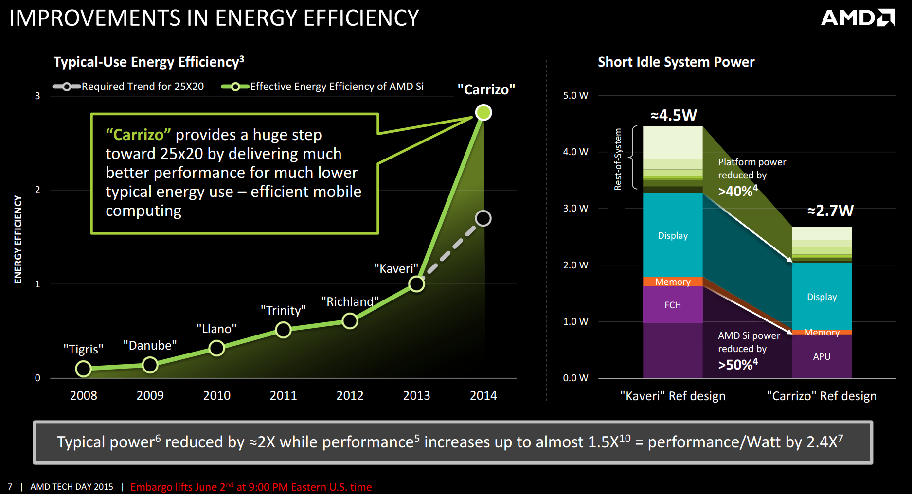
Ultimately this all helps AMD’s plan to be 25x more efficient with their APUs by 2020, and the cumulative bar chart on the right is how mobile improvements from all sides are being realized. Migrating the southbridge on die severely reduces its idle power consumption to almost zero and can help efficiencies elsewhere in the system. The APU general use and memory controllers are the next targets, but the common constant here is the display. Using a low power display might give battery life in exchange for quality, and there is only so much power you can save at the SoC level. In time, the display will be the main focus of power saving for these devices.
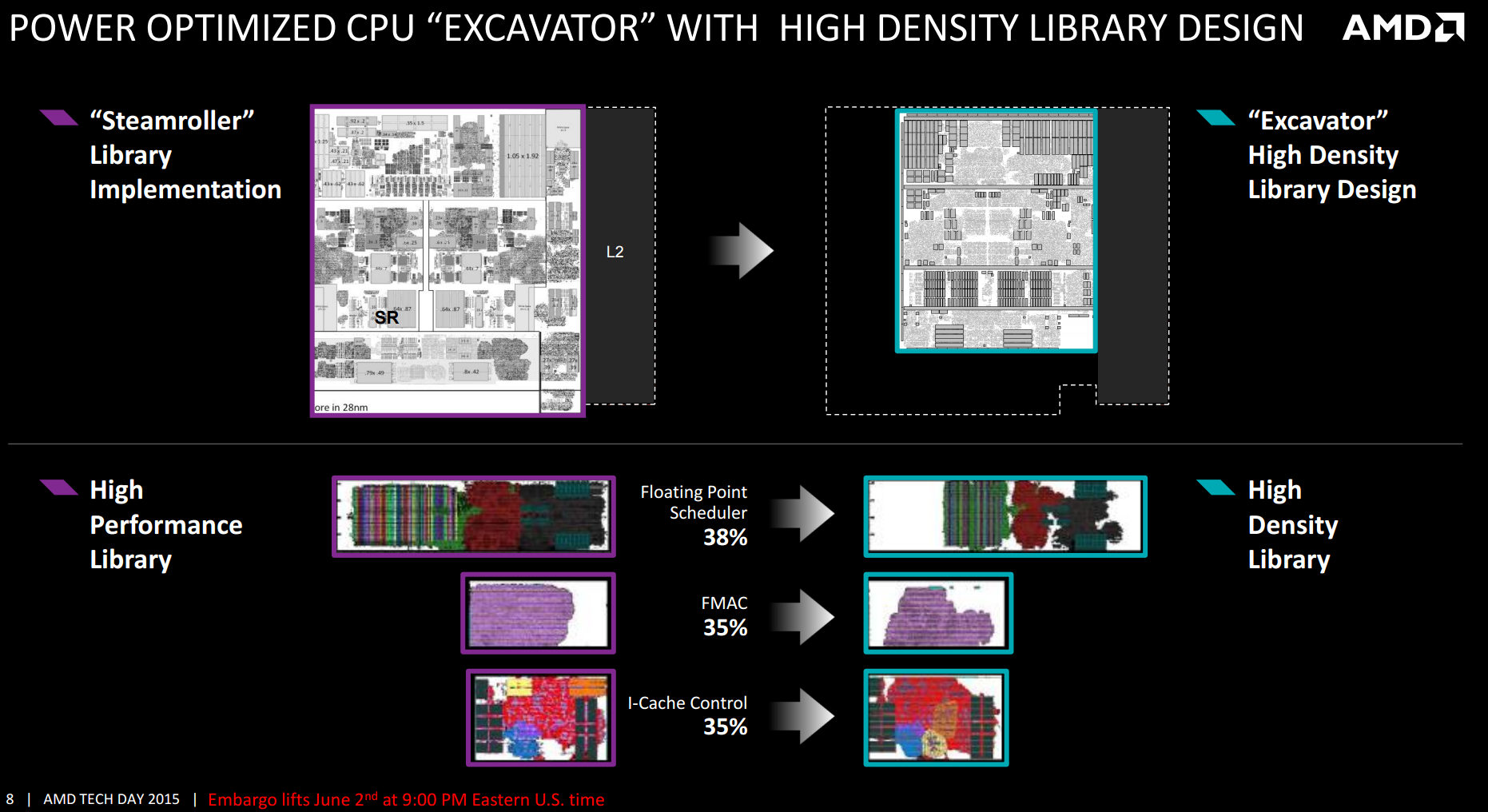
A big part of the reduction in die area comes from the set of high density libraries being used by AMD. Above were three examples provided where >33% gains were made in silicon area. Typically using a high density library design is a double edged sword – it reduces die area and potentially leaves more area for other things, but the caveat is that it may be more prone to defects in construction, require additional latency or have a different frequency/voltage profile. AMD assures us that these changes are at least like-for-like but most of them contain other improvements as well.
It’s worth noting here that AMD has described the high density library project internally as the equivalent of a moonshot, essentially the developers were part of a ‘skunkworks’ division attempting to make drastic changes in order to improve performance. The high density library is one such successful project from that.
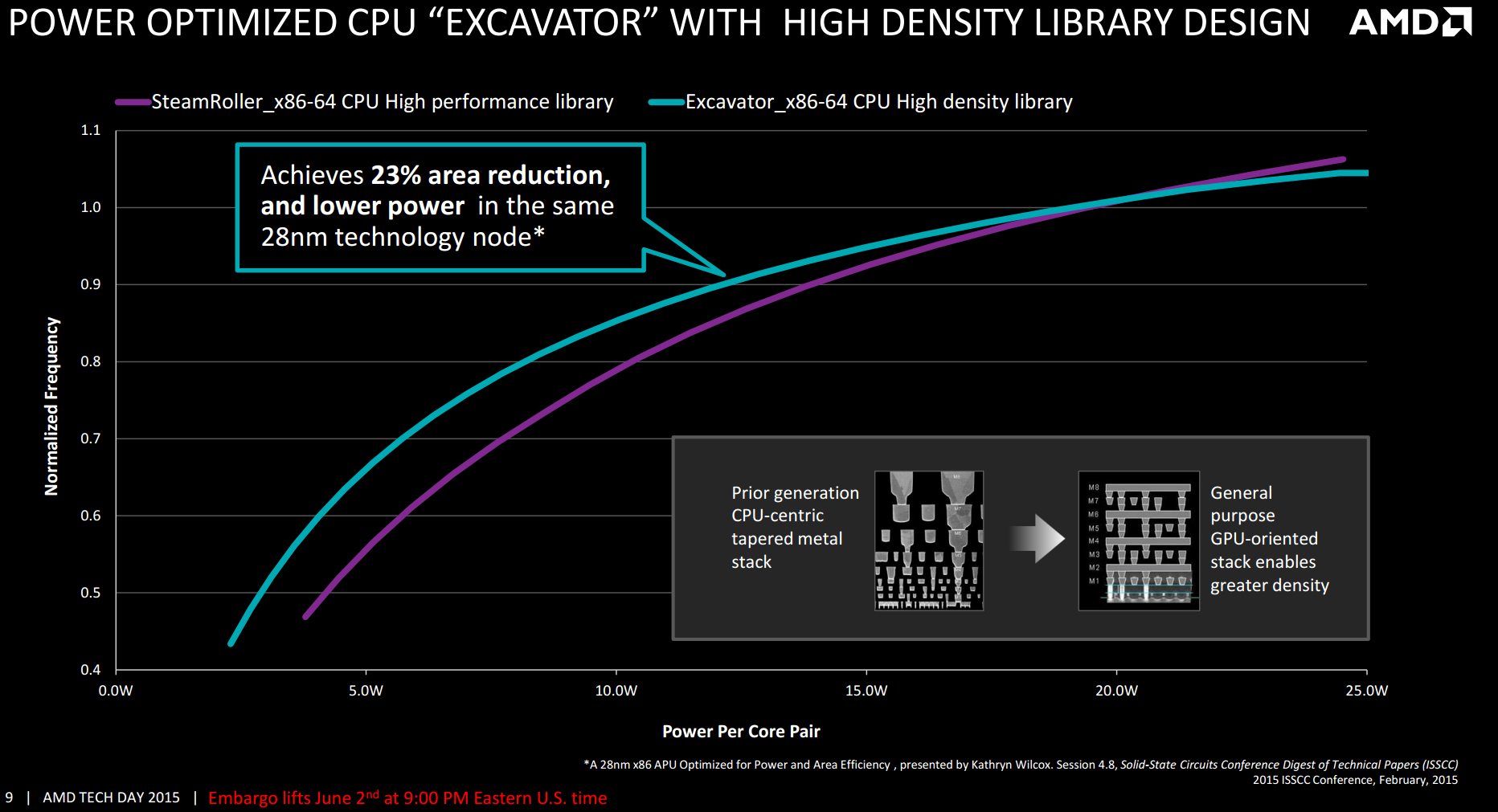
With the new libraries, comparing Excavator to Steamroller shows the effect moving designs has. The power/frequency curve below 20W per module shifts to higher frequency/lower power, whereas losses are observed above 20W. However for 15W per module, this means either a 10%+ power reduction at the same frequency or a 5% increase in frequency for the same power. Should AMD release dual thread / single core APUs in the 7.5W region, this is where most of the gains are (as noted in the comments, the dual module designs are at 7.5W per module, meaning that what we should see in devices is already in the peak value for gains and benefits such as 25% frequency or 33% power). As also seen in the insert, the silicon stack has been adjusted to a more general purpose orientation. I could comment that this makes the CPU and GPU work better together, but I have no way of verifying this. AMD states the change in the silicon stack makes production slightly easier but also helps with achieving the higher density Excavator exhibits.


137 Comments
View All Comments
name99 - Saturday, June 6, 2015 - link
You are comparing a $400 laptop to a $1500 laptop and, what do you know, the $1500 laptop comes out better. What a surprise!The point is that in this space batteries have long been cheap and the energy efficiency nothing like at the higher end. Which means the work-life has been something like 3 hrs. If AMD shifts that to six hours with this chip, that's a massive improvement in the target space.
You're also making bad assumptions about why these laptops are bought. If you rely on your laptop heavily for your job, you buy a $1500 laptop. These machines are bought to act as light performance desk machines that are occasionally (but only occasionally) taken to a conference room or on a field trip.
name99 - Saturday, June 6, 2015 - link
AMD does not have infinite resources. This play makes sense.Intel is essentially operating by starting with a Xeon design point and progressively stripping things out to get to Broadwell-M, which means that Broadwell-M over-supplies this $400-$700 market. Meanwhile at the really low end, Intel has Atom.
AMD is seeing (correctly, I think) that there is something of a gap in the Intel line which they can cover AND that this gap will probably persist for some time --- Intel isn't going to create a third line just to fit that gap.
Krysto - Wednesday, June 3, 2015 - link
I might be ready to get into AMD, as AMD has a lot of innovation lately. But it still disappoints me greatly that they aren't able to adopt a more modern process node.If they launch their new high-performance CPU core next year as part of an APU that uses HBM memory and is at the very least on 16nm FinFET, I might get that instead of a Skylake laptop. HSA is pretty cool and one of the reasons I'd get it.
UtilityMax - Wednesday, June 3, 2015 - link
The Kaveri FX parts are still almost half as slow in IPC as a competing Intel Core i3 with the same TDP. Only in tests involving multithreaded apps that can load all four cores the FX parts are keeping up with the Core i3. Let's hope the Carrizo generation of APUs will improve this situation.silverblue - Thursday, June 4, 2015 - link
Without being an AMD apologist, I think the point was that single threaded performance was "good enough" for your usual light work which tends to be hamstrung by I/O anyway.There are two things that I need to see clarified about Carrizo, however:
1) Does Carrizo drop CPU frequency automatically when the GPU is being taxed? That's certainly going to be an issue as regards the comparison with an i3.
2) With the addition of AVX2, were there any architectural changes made to accommodate AVX2, for example a wider FlexFPU?
sonicmerlin - Tuesday, June 9, 2015 - link
Yup. I'll wait for the 14 nm Zen APUs with HBM. The performance leap (both CPU and GPU) should be truly massive.Phartindust - Thursday, June 4, 2015 - link
Dude your gettin a Dell with a AMD processor!When was the last time that happened?
Looks like @Dell loves #Carrizo, and will use @AMD once again. #AMDRTP http://www.cnet.com/au/news/dell-inspirion-amd-car... …
elabdump - Friday, June 5, 2015 - link
Don't forget that Intel gives you an non fixable NSA approved BIOS: http://mjg59.dreamwidth.org/33981.htmlpatrickjchase - Friday, June 5, 2015 - link
Ian, you appear to have confused I-cache and D-cache.You wrote: "The L1 data cache is also now an 8-way associative design, but with the better branch prediction when needed it will only activate the one segment required and when possible power down the rest".
This is of course gibberish. Branch prediction would help to predict the target set of an *instruction* fetch from the I-cache, but is useless for D-cache set prediction for the most part (I say "for the most part" because Brad Calder did publish a way-prediction scheme based on instruction address back in the 90s. It didn't work very well and hasn't been productized that I know of).
zodiacfml - Friday, June 5, 2015 - link
Imagine what they could with 14nm of this, probably at half the cost of a Core M with 60 to 70% CPU performance of the M, yet with better graphics at the same TDP.