AMD Launches Carrizo: The Laptop Leap of Efficiency and Architecture Updates
by Ian Cutress on June 2, 2015 9:00 PM ESTEfficiency and Die Area Savings
AMD’s take home message in all of this is efficiency. We a being quoted a performance per watt increase of 2.4x, coming from typical power draw savings of 2x and performance increase of almost 1.5x for 23% less die area, all in one go.
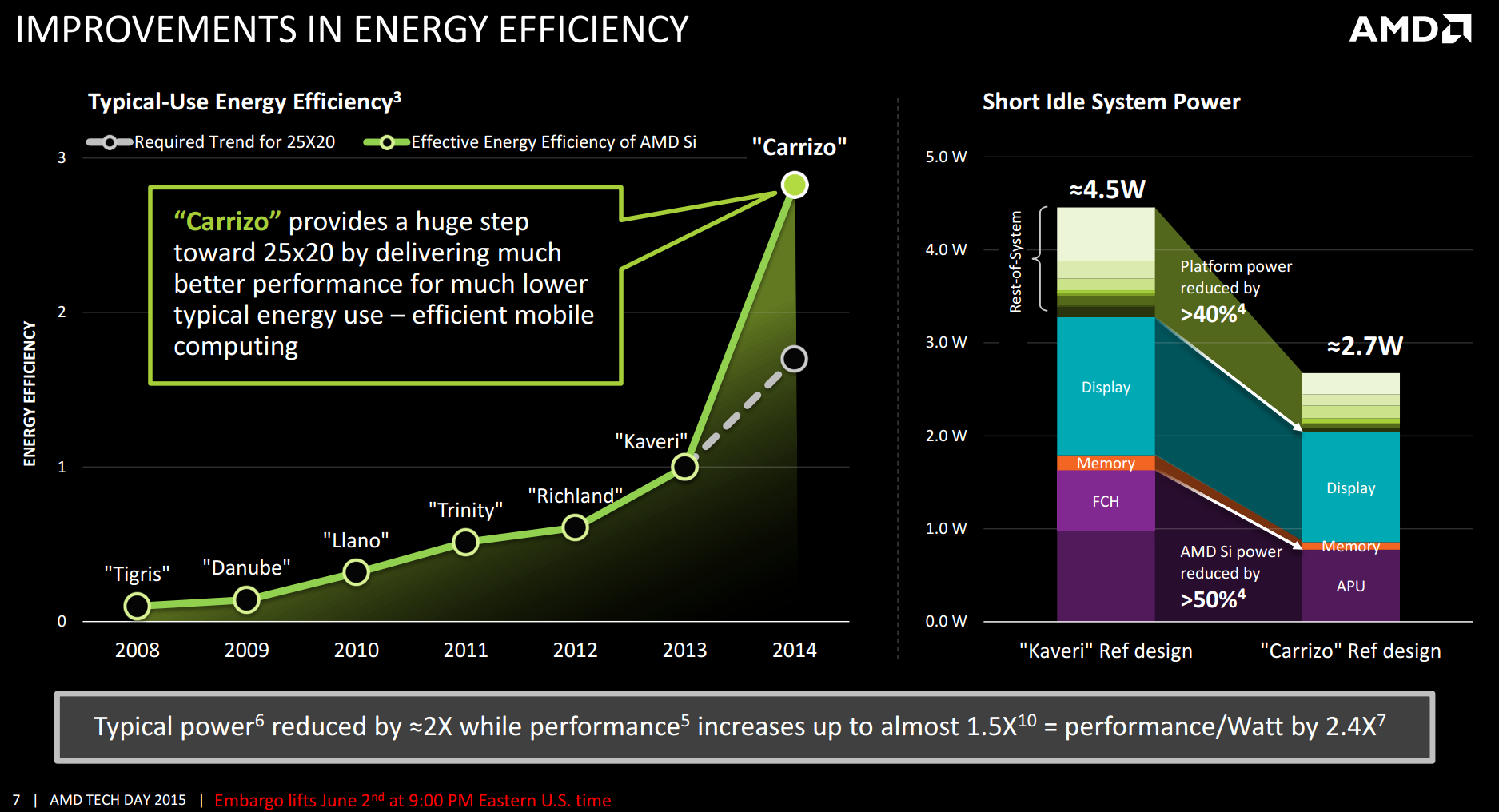
Ultimately this all helps AMD’s plan to be 25x more efficient with their APUs by 2020, and the cumulative bar chart on the right is how mobile improvements from all sides are being realized. Migrating the southbridge on die severely reduces its idle power consumption to almost zero and can help efficiencies elsewhere in the system. The APU general use and memory controllers are the next targets, but the common constant here is the display. Using a low power display might give battery life in exchange for quality, and there is only so much power you can save at the SoC level. In time, the display will be the main focus of power saving for these devices.
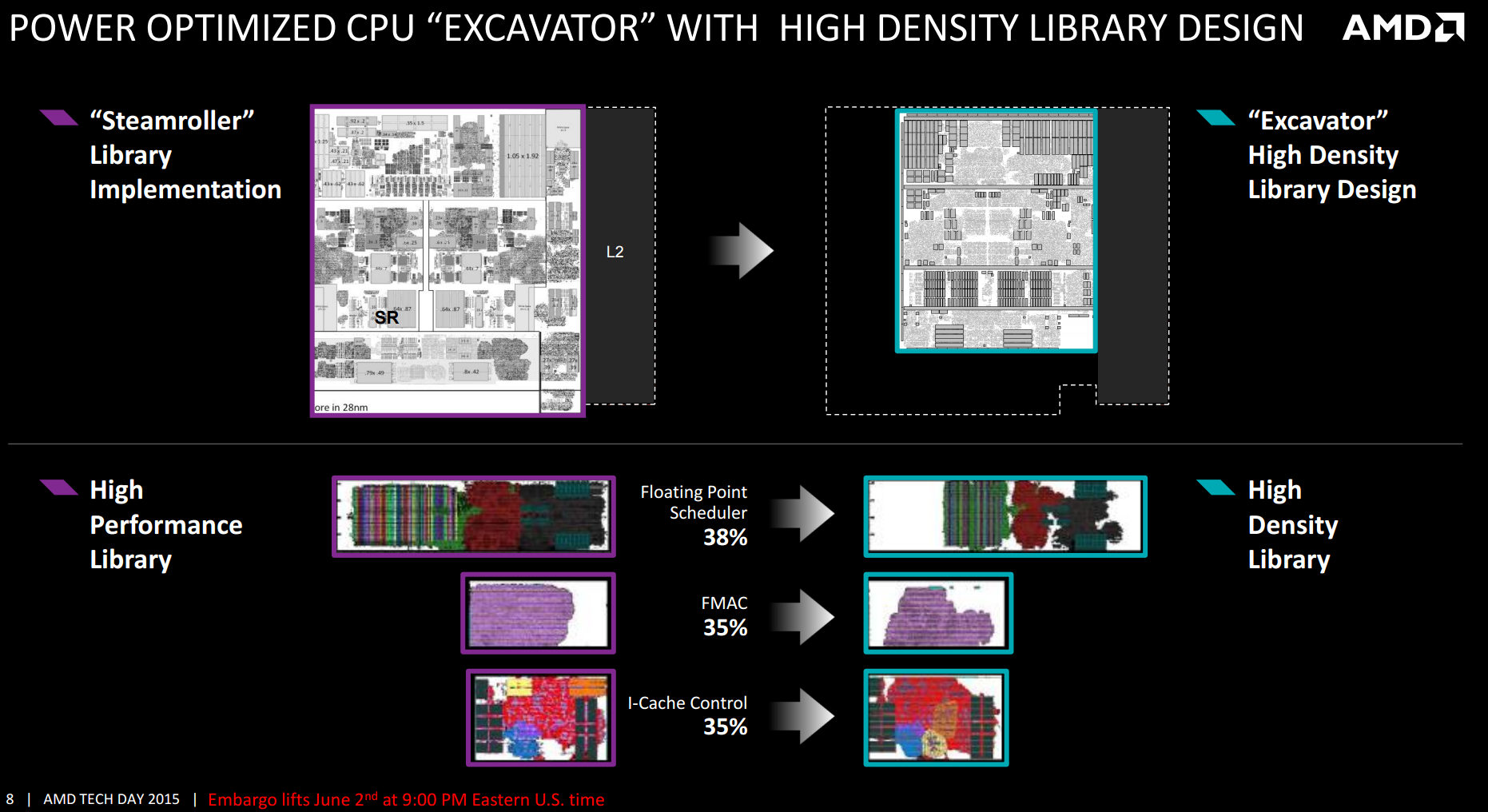
A big part of the reduction in die area comes from the set of high density libraries being used by AMD. Above were three examples provided where >33% gains were made in silicon area. Typically using a high density library design is a double edged sword – it reduces die area and potentially leaves more area for other things, but the caveat is that it may be more prone to defects in construction, require additional latency or have a different frequency/voltage profile. AMD assures us that these changes are at least like-for-like but most of them contain other improvements as well.
It’s worth noting here that AMD has described the high density library project internally as the equivalent of a moonshot, essentially the developers were part of a ‘skunkworks’ division attempting to make drastic changes in order to improve performance. The high density library is one such successful project from that.
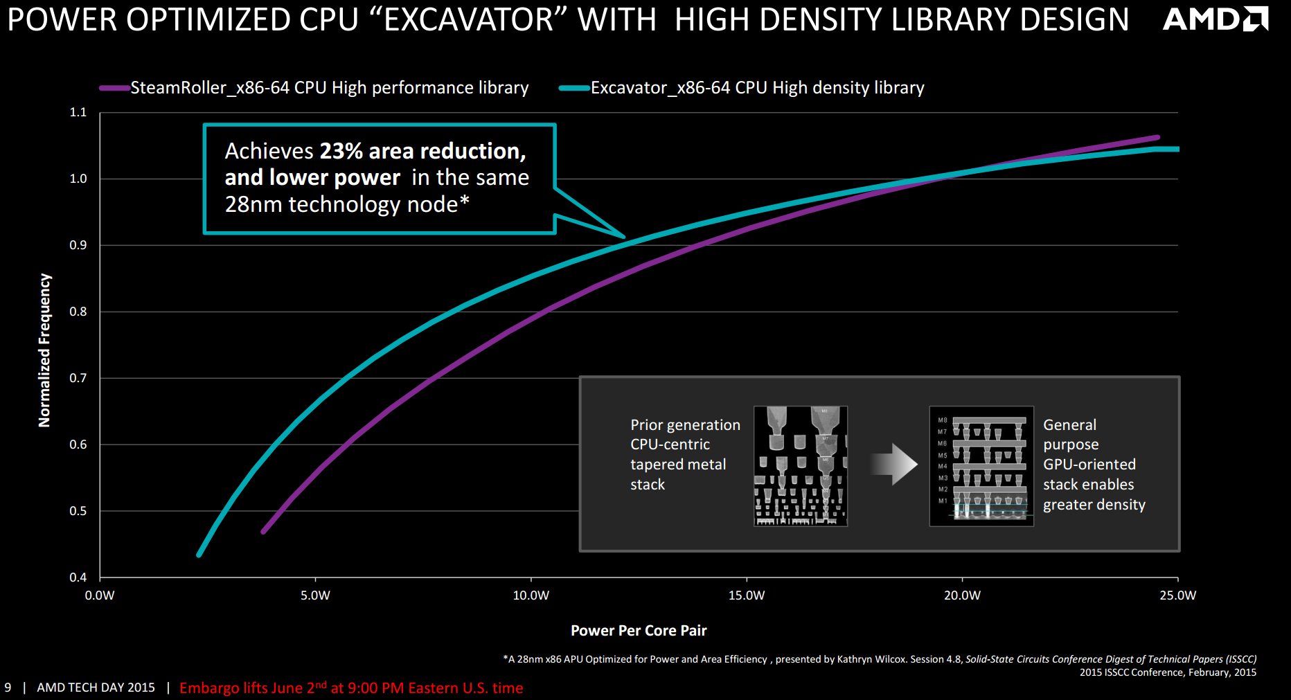
With the new libraries, comparing Excavator to Steamroller shows the effect moving designs has. The power/frequency curve below 20W per module shifts to higher frequency/lower power, whereas losses are observed above 20W. However for 15W per module, this means either a 10%+ power reduction at the same frequency or a 5% increase in frequency for the same power. Should AMD release dual thread / single core APUs in the 7.5W region, this is where most of the gains are (as noted in the comments, the dual module designs are at 7.5W per module, meaning that what we should see in devices is already in the peak value for gains and benefits such as 25% frequency or 33% power). As also seen in the insert, the silicon stack has been adjusted to a more general purpose orientation. I could comment that this makes the CPU and GPU work better together, but I have no way of verifying this. AMD states the change in the silicon stack makes production slightly easier but also helps with achieving the higher density Excavator exhibits.


137 Comments
View All Comments
VeixES - Wednesday, June 3, 2015 - link
Some OEM needs to pick this up fast.Carrizo based "NUC" device with HDMI2.0 output with more barebones approach than intel to reduce the cost of entry.
gostan - Wednesday, June 3, 2015 - link
Anandtech - AMD's marketing arm.bloodypulp - Wednesday, June 3, 2015 - link
Dumbest thing I've heard yet today.jabber - Thursday, June 4, 2015 - link
Everyone knows AMD has never had a marketing arm. That's why no one buys em.Seriously, the OEMs have moved on. Why bother with AMD when Intel sells because the average consumer has heard of Intel? Price doesn't come into it.
watzupken - Thursday, June 11, 2015 - link
To gostan, I find your comment above baseless and unconstructive to be honest. One article on AMD means AMD marketing arm. So what does that make you then?l_d_allan - Wednesday, June 3, 2015 - link
My impression is that it will be difficult (almost impossible?) for AMD to compete with a 28nm part against Intel's 14nm parts.And I think the next "tick tock" from Intel will be 10nm. Or not?
Novacius - Wednesday, June 3, 2015 - link
It'll be a tick, codenamed Cannonlake. But i don't expect it before the end of 2016/beginning of 2017.The_Assimilator - Wednesday, June 3, 2015 - link
Which will still be before AMD gets to 14nm.cjs150 - Wednesday, June 3, 2015 - link
Finally AMD release a reasonably power efficient chip.At 15W this is perfect for a passively cooled HTPC with 4k capability built in. I appreciate the HTPC market is small, but AMD have something that potentially (will reserve judgment until it is out and tested) beats everything Intel have comprehensively.
The problem for AMD will be that people like me already have a HTPC (in my case using i7-3770T which is overkill) and until the world moves to 4K there is no need to upgrade but if they produced something the size of Intel NUC but passively cooled I would be very tempted
watzupken - Wednesday, June 3, 2015 - link
I think this makes a very interesting APU. In fact, the most interesting APU from AMD to date. Unfortunately, it may not reach the shores from where I come from. It is either limited availability or the distros are not interested to carry in due to them expecting a low demand.