AMD Dives Deep On High Bandwidth Memory - What Will HBM Bring AMD?
by Ryan Smith on May 19, 2015 8:40 AM ESTThe Net Benefits of HBM
Now that we’ve had a chance to talk about how HBM is constructed and the technical hurdles in building it, we can finally get to the subject of the performance and design benefits of HBM. HBM is of course first and foremost about further increasing memory bandwidth, but the combination of stacked DRAM and lower power consumption also opens up some additional possibilities that could not be pursued with GDDR5.
We’ll start with the bandwidth capabilities of HBM. The amount of bandwidth ultimately depends on the number of stacks in use along with the clockspeed of those stacks. HBM uses a DDR signaling interface, and while AMD is not disclosing final product specifications at this time, they have given us enough information to begin to build a complete picture.
| GPU Memory Math | |||||
| AMD Radeon R9 290X | NVIDIA GeForce GTX Titan X | Theoretical 4-Stack HBM1 | |||
| Total Capacity | 4GB | 12GB | 4GB | ||
| Bandwidth Per Pin | 5Gbps | 7Gbps | 1Gbps | ||
| Number of Chips/Stacks | 16 | 24 | 4 | ||
| Bandwidth Per Chip/Stack | 20GB/sec | 14GB/sec | 128GB/sec | ||
| Effective Bus Width | 512-bit | 384-bit | 4096-bit | ||
| Total Bandwidth | 320GB/sec | 336GB/sec | 512GB/sec | ||
| Estimated DRAM Power Consumption |
30W | 31.5W | 14.6W | ||
The first generation of HBM AMD is using allows for each stack to be clocked up to 500MHz, which after DDR signaling leads to 1Gbps per pin. For a 1024-bit stack this means a single stack can deliver up to 128GB/sec (1024b * 1G / 8b) of memory bandwidth. HBM in turn allows from 2 to 8 stacks to be used, with each stack carrying 1GB of DRAM. AMD’s example diagrams so far (along with NVIDIA’s Pascal test vehicle) have all been drawn with 4 stacks, in which case we’d be looking at 512GB/sec of memory bandwidth. This of course is quite a bit more than the 320GB/sec of memory bandwidth for the R9 290X or 336GB/sec for NVIDIA’s GTX titan X, working out to a 52-60% increase in memory bandwidth.
At the same time this also calls into question memory capacity – 4 1GB stacks is only 4GB of VRAM – though AMD seems to be saving that matter for the final product introduction later this quarter. Launching a new, high-end GPU with 4GB could be a big problem for AMD, but we'll see just what they have up their sleeves in due time.
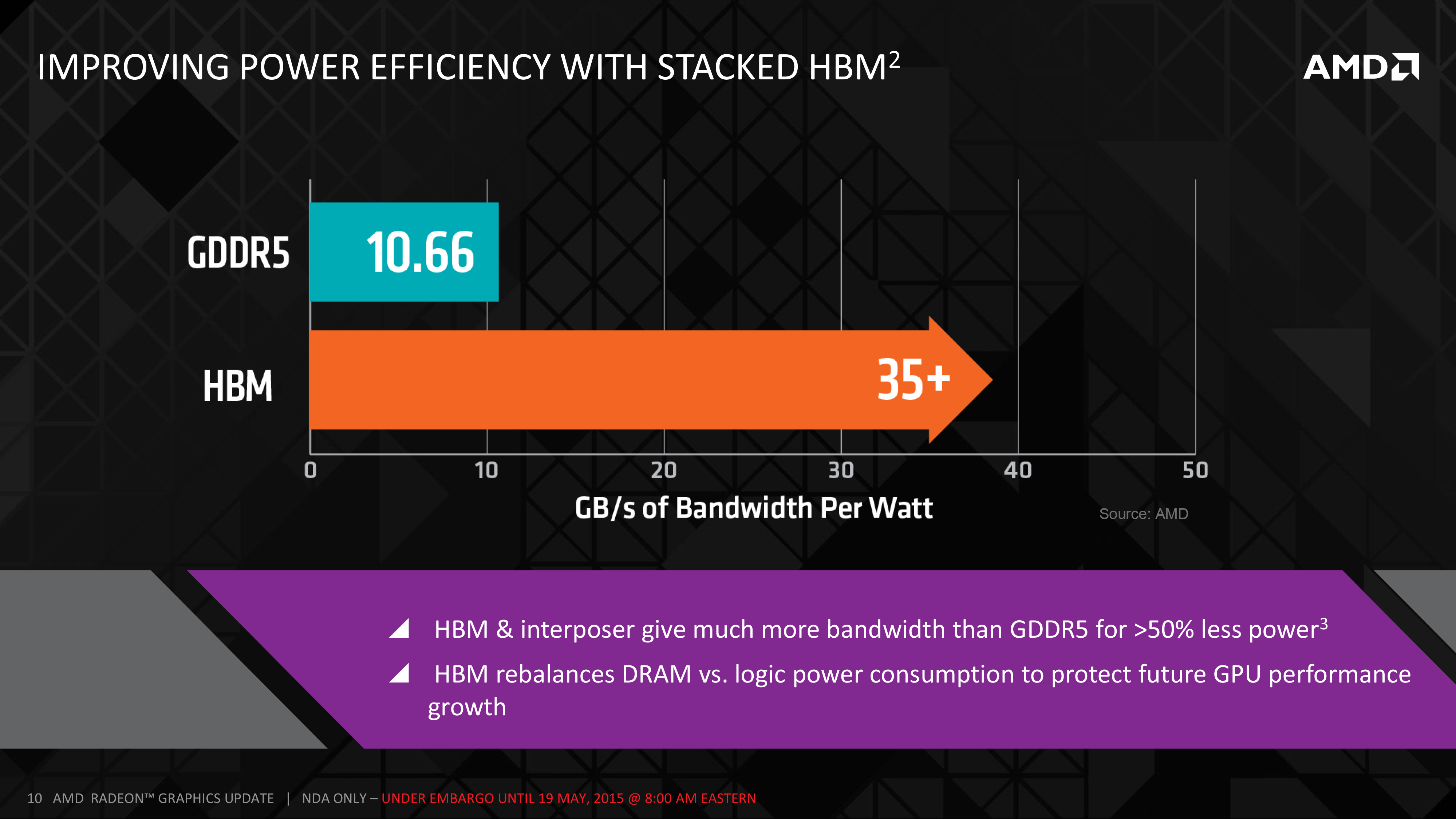
What’s perhaps more interesting is what happens to DRAM energy consumption with HBM. As we mentioned before, R9 290X spends 15-20% of its 250W power budget on DRAM, or roughly 38-50W of power on an absolute basis. Meanwhile by AMD’s own reckoning, GDDR5 is good for 10.66GB/sec of bandwidth per watt of power, which works out to 30W+ via that calculation. HBM on the other hand delivers better than 35GB/sec of bandwidth per watt, an immediate 3x gain in energy efficiency per watt.
Of course AMD is then investing some of those gains back in to coming up with more memory bandwidth, so it’s not as simple as saying that memory power consumption has been cut by 70%. Rather given our earlier bandwidth estimate of 512GB/sec of memory bandwidth for a 4 stack configuration, we would be looking at about 15W of power consumption for a 512GB/sec HBM solution, versus 30W+ for a 320GB/sec GDDR5 solution. The end result then points to DRAM power consumption being closer to halved, with AMD saving 15-20W of power.
What’s the real-world advantage of a 15-20W reduction in DRAM power consumption? Besides being able to invest that in reducing overall video card power consumption, the other option is to invest it in increasing clockspeeds. With PowerTune putting a hard limit on power consumption, a larger GPU power budget would allow AMD to increase clockspeeds and/or run at the maximum GPU clockspeed more often, improving performance by a currently indeterminable amount. Now as fair warning here, higher GPU clockspeeds typically require higher voltages, which in turn leads to a rapid increase in GPU power consumption. So although having additional power headroom does help the GPU, it may not be good for quite as much of a clockspeed increase as one might hope.
Meanwhile the performance increase from the additional memory bandwidth is equally nebulous until AMD’s new product is announced and benchmarked. As a rule of thumb GPUs are virtually always memory bandwidth bottlenecked – they are after all high-throughput processors capable of trillions of calculations per second working with only hundreds of billions of bytes of bandwidth – so there is no doubt that the higher memory bandwidths of HBM will improve performance. However memory bandwidth increases currently don’t lead to 1:1 performance increases even on AMD’s current cards, and it’s unlikely to be any different on future products.
Throwing an extra wrinkle into matters, any new AMD product would be based on GCN 1.2 or newer, which introduced AMD’s latest generation of color compression technology. The net result is that on identical workloads, memory bandwidth pressure is going down exactly at the same time as memory bandwidth availability is going up. AMD will end up gaining a ton of effective memory bandwidth – something that will be very handy for high resolutions – but it also makes it impossible to predict what the final performance impact might be. Still, it will be interesting to see what AMD can do with a 2x+ increase in effective memory bandwidth for graphics workloads.
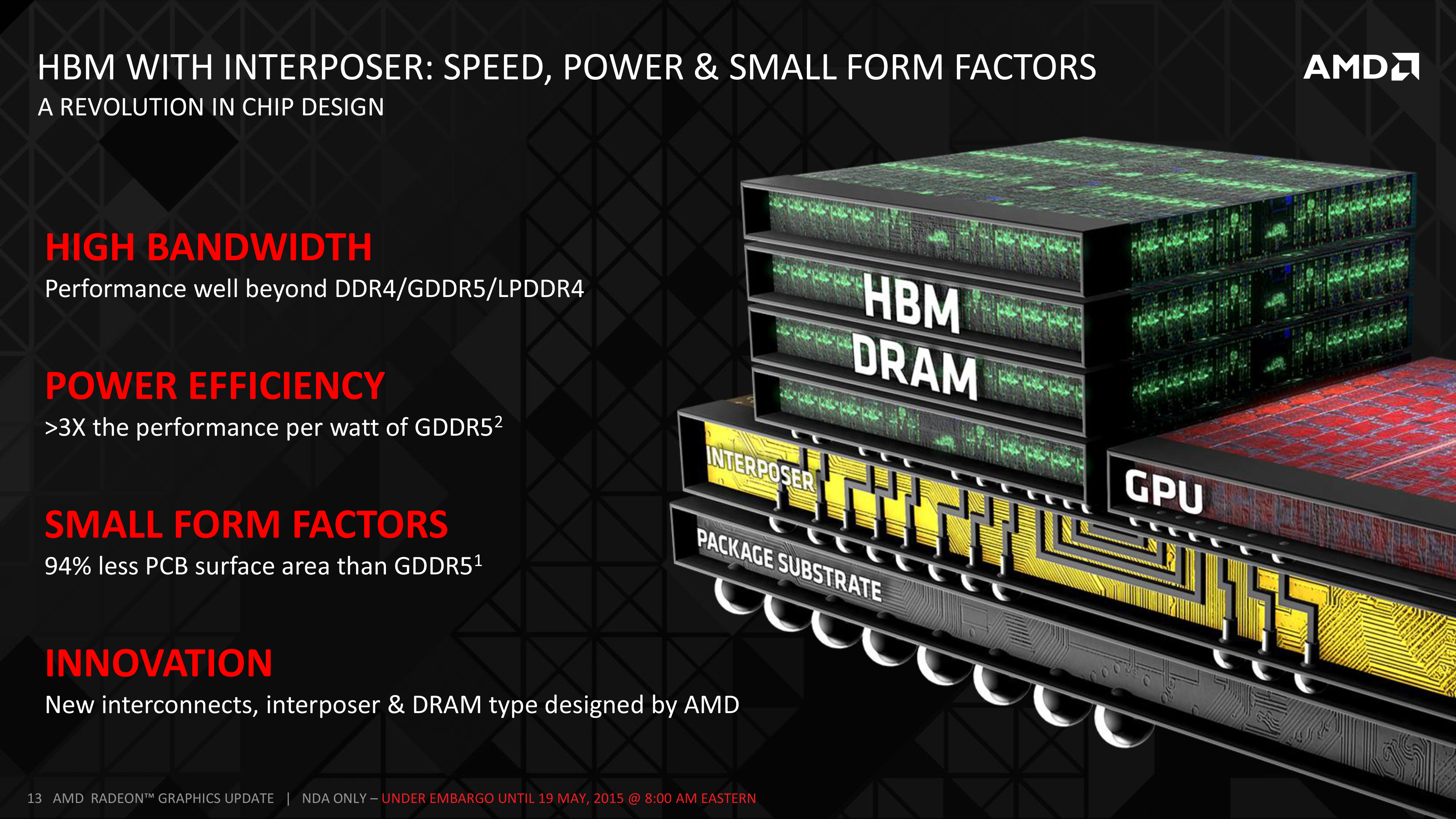
The final major benefit AMD is looking at taking advantage of with HBM – and that this point they’re not even being subtle about – is new form factor designs from the denser designs enabled by HBM. With the large GDDR5 memory chips replaced with much narrower HBM stacks, AMD is telling us that the resulting ASIC + RAM setups can be much smaller.
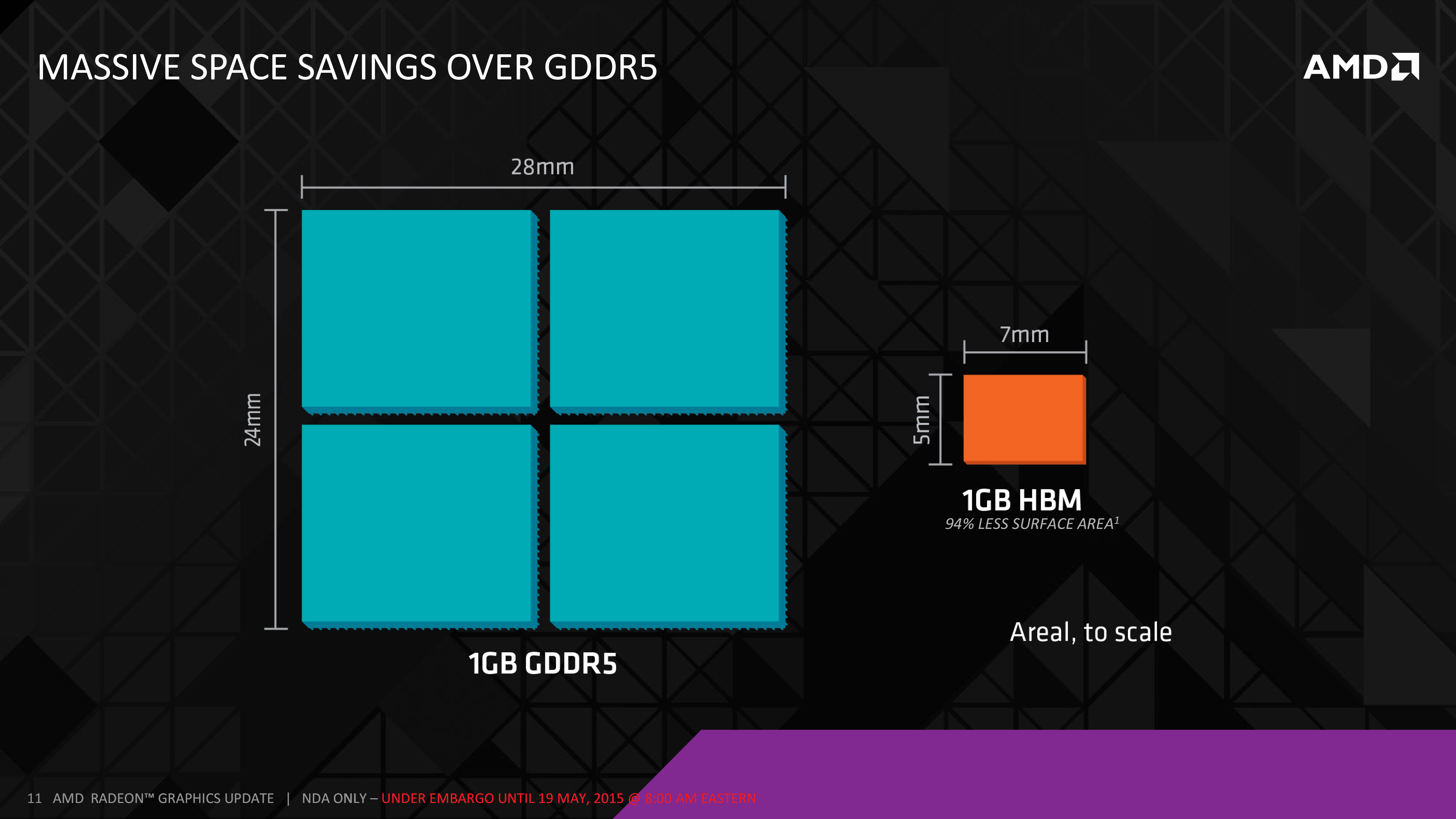
How much smaller? Well 1GB of GDDR5, composed of 2Gbit modules (the standard module size for R9 290X) would take up 672mm2, versus just 35mm2 for the same 1GB of DRAM as an HBM stack. Even if we refactor this calculation for 4Gbit modules – the largest modules used in currently shipping video cards – then we still end up with 336mm2 versus 35mm2, which is still a savings of 89% for 1GB of DRAM. Ultimately the HBM stack itself is composed of multiple DRAM dies, so there’s still quite a bit of silicon in play, however its 2D footprint is reduced significantly thanks to stacking.
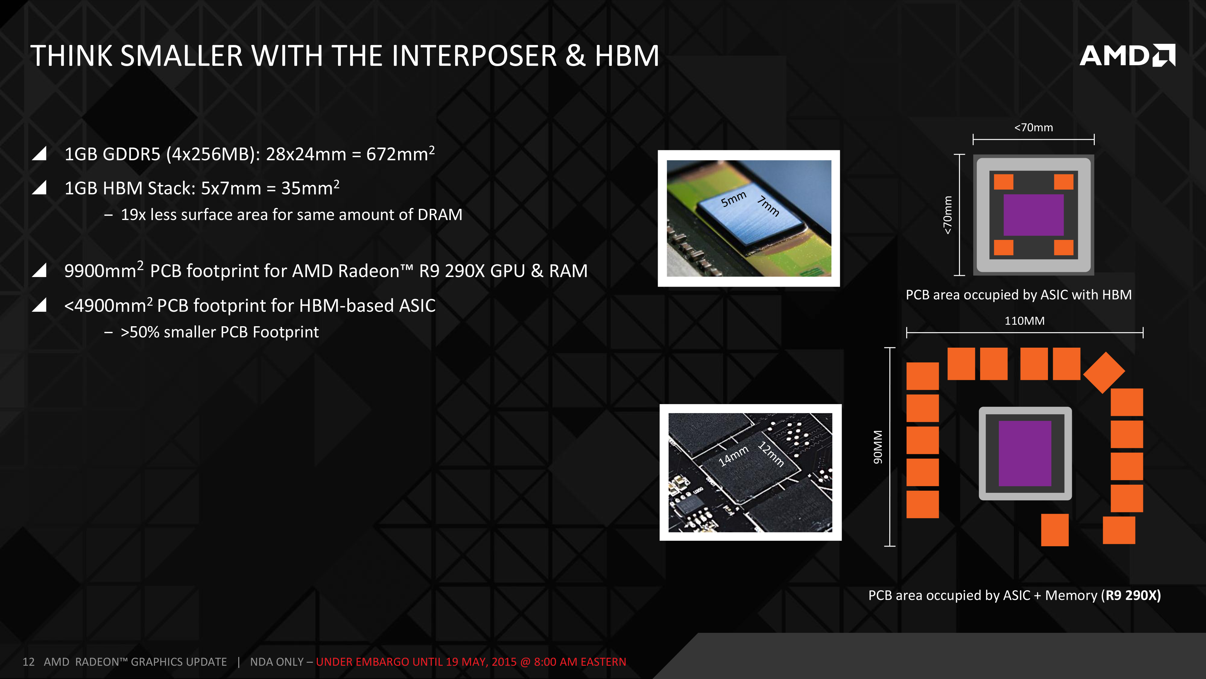
By AMD’s own estimate, a single HBM-equipped GPU package would be less than 70mm X 70mm (4900mm2), versus 110mm X 90mm (9900mm2) for R9 290X. Throw in additional space savings from the fact that HBM stacks don’t require quite as complex power delivery circuitry, and the card space savings could be significant. By our reckoning the total card size will still be fairly big – all of those VRMs and connectors need to go somewhere – but there is potential for significant savings. What AMD intends to do with those savings remains to be seen, but with apologies to AMD on this one, NVIDIA has already shown off their Pascal test vehicle for their mezzanine connector design, and it goes without saying that such a form factor opens up some very interesting possibilities.
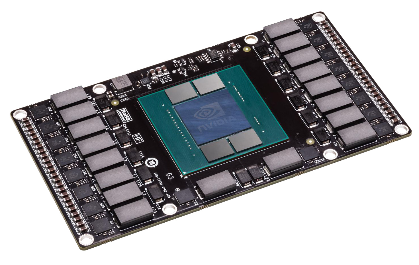
With apologies to AMD: NVIDIA’s Pascal Test Vehicle, An Example Of A Smaller, Non-Traditional Video Card Design
Finally, aftermarket enthusiasts may or may not enjoy one final benefit from the use of HBM. Because the DRAM and GPU are now on the same package, AMD is going to be capping the package with an integrated heat spreader (IHS) to compensate for any differences in height between the HBM stacks and GPU die, to protect the HBM stacks, and to supply the HBM stacks with sufficient cooling. High-end GPU dies have been bare for some time now, so an IHS brings with it the same kind of protection for the die that IHSs brought to CPUs. At the same time however this means it’s no longer possible to make direct contact with the GPU, so extreme overclockers may come away disappointed. We’ll have to see what the shipping products are like and whether in those cases it’s viable to remove the IHS.
Closing Thoughts
Bringing this deep dive to a close, as the first GPU manufacturer to be shipping an HBM solution – in fact AMD expects to be the only vendor to ship an HBM1 solution – AMD has set into motion some very aggressive product goals thanks to the gains from HBM. Until we know more about AMD’s forthcoming video card I find it prudent to keep expectations in check here, as HBM is just one piece of the complete puzzle that is a GPU. But at the same time let’s be clear here: HBM is the future memory technology of GPUs, there is potential for significant performance increases thanks to the massive increase in memory bandwidth offers, and for roughly the next year AMD is going to be the only GPU vendor offering this technology.
AMD for their part is looking to take as much of an advantage of their lead as they can, both at the technical level and the consumer level. At the technical level AMD has said very little about performance so far, so we’ll have to wait and see just what their new product brings. But AMD is being far more open about their plans to exploit the size advantage of HBM, so we should expect to see some non-traditional designs for high-end GPUs. Meanwhile at the consumer level, expect to see HBM enter the technology lexicon as the latest buzzword for high-performance products – almost certainly to be stamped on video card boxes today just as GDDR5 has been for years – as AMD looks to let everyone know about their advantage.
Meanwhile shifting gears towards the long term, high-end GPUs are just the first of what AMD expects to be a wider rollout for HBM. Though AMD is not committing to any other products at this time, as production ramps up and costs come down, HBM is expected to become financially viable in a wider range, including lower-end GPUs, HPC products (e.g. FirePro S and AMD’s forthcoming HPC APU), high-end communications gear, and of course AMD’s mainstream consumer APUs. As lower-margin products consumer APUs will likely be among the farthest off, however in the long-run they may very well be the most interesting use case for HBM, as APUs are among the most bandwidth-starved graphics products out there. But before we get too far ahead of ourselves, let’s see what AMD is able to do with HBM on their high-end video cards later this quarter.


163 Comments
View All Comments
testbug00 - Tuesday, May 19, 2015 - link
Name long term good relationships that Nvidia has had with other companies in the industry. Besides their board partners. You could argue TSMC either way. Otherwise, I'm getting nothing. They recently have a relationship with IBM that could become long term. It is entirely possible I'm just missing the companies they partner with that are happy with their partnership in the semi-conductor industry.Compared to IBM, TSMC, SK Hynix, and more.
ImSpartacus - Tuesday, May 19, 2015 - link
Can we have an interview with Joe Macri? He seems like a smart fella if he was the primary reference for this article.wnordyke - Tuesday, May 19, 2015 - link
This analysis does not discuss the benefits of the base die? The base die contains the memory controller and a data serializer. The architecture of moving the memory controller to the base die simplifies the design and removes many bottlenecks. The Base die is large enough to support a large number of circuits. (#1 memory controller, #2 Cache, #3 data processing)The 4096 wires is a large number and 4096 I/O buffers is a large number. The area of 4096 I/O buffers on the GPU die is expensive, and this expense is easily avoided by placing the memory controller on the base die. The 70% memory Bus efficiency is idle bandwidth, and this idle data does not need to be sent back to the GPU. The 4096 Interposer signals reduces to (4096 * 0.7 = 2867) saving 1,229 wires + I/O buffers.
A simple 2 to 1 serializer would reduces down to (2867 * 0.50 = 1432). The Interposer wires are short enough to avoid the termination resistors for a 2GHz signal. Removing the termination resistors is top of the list to saving power, the second on the list to save power is to minimize the Row Activate.
takeship - Tuesday, May 19, 2015 - link
So am I correct in assume then that the 295x2 equivalent performance numbers for Fiji leaked months ago are for the dual gpu variant? It concerns me that at no point in this write up did AMD even speculate what the performance inc with HBM might be.dew111 - Tuesday, May 19, 2015 - link
Why is everyone concerned about the 4GB limit in VRAM? A few enthusiasts might be disappointed, but for anyone who isn't using multiple 4k monitors, 4GB is just fine. It might also be limiting in some HPC workloads, but why would any of us consumers care about that?chizow - Wednesday, May 20, 2015 - link
I guess the concern is that people were expecting AMD's next flagship to pick up where they left off on the high-end, and given how much AMD has touted 4K, that would be a key consideration. Also, there are the rumors this HBM part is $850 to create a new AMD super high-end, so yeah, if you're going to say 4K is off the table and try to sell this as a super premium 4K part, you're going to have a hard sell as that's just a really incongruent message.In any case, AMD says they can just driver-magic this away, which is a recurring theme for AMD, so we will see. HBM's main benefits are VRAM to GPU transfers, but anything that doesn't fit in the local VRAM are still going to need to come from System RAM or worst, local storage. Textures for games are getting bigger than ever...so yeah not a great situation to be stuck at 4GB for anything over 1080p imo.
zodiacfml - Tuesday, May 19, 2015 - link
Definitely for their APUs and mobile. Making this first on GPUs helps recover the R&d without the volume scale.SolMiester - Tuesday, May 19, 2015 - link
Do the R9 290\x really perform that much better with OC memory on the cards? I didnt think AMD was ever really constrained by bandwidth, as they usually always had more on their generation of cards.Consequently, I dont see 390\x being that much competition to Titan X
Intel999 - Tuesday, May 19, 2015 - link
Thanks SolMiester,You have done an excellent job of displaying your level of intelligence. I don't think the New York Giants will provide much competition to the rest of the NFL this year. I won't support my prediction with any facts or theories just wanted to demonstrate that I am not a fan of the Giants.
BillyHerrington - Tuesday, May 19, 2015 - link
Since HBM are owned by AMD & Hynix, does other company (nvidia, etc) have to pay AMD in order to use HBM tech ?