The Intel Xeon E7-8800 v3 Review: The POWER8 Killer?
by Johan De Gelas on May 8, 2015 8:00 AM EST- Posted in
- CPUs
- IT Computing
- Intel
- Xeon
- Haswell
- Enterprise
- server
- Enterprise CPUs
- POWER
- POWER8
Xeon E7 v3 System and Memory Architecture
So, the Xeon E5 "Haswell EP" and Xeon E7 "Haswell EX" are the same chip, but the latter has more features enabled and as result it finds a home in a different system architecture.
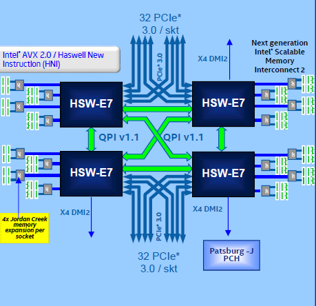
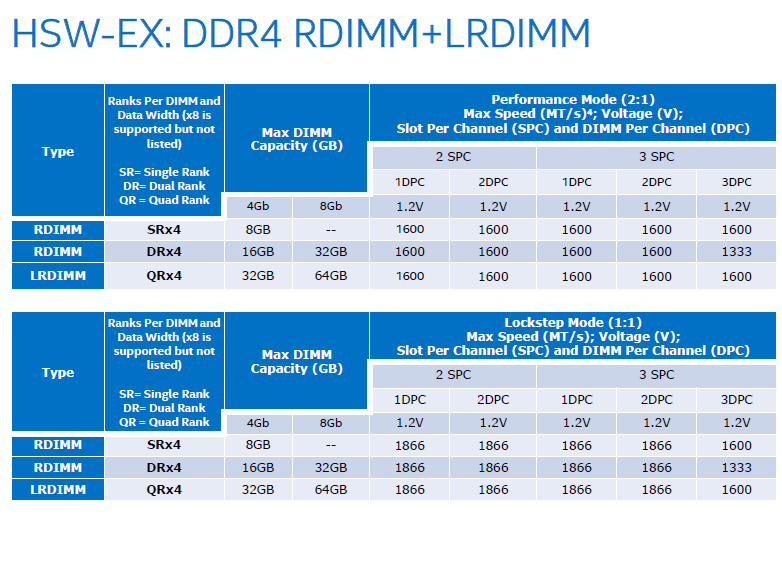
Debuting alongside the Xeon E7 v3 is the new "Jordan Creek 2" buffer chip, which offers support for DDR4 LR-DIMMs or buffered RDIMMs. However if necessary it is still possible to use the original "Jordan Creek" buffer chips with DDR3, giving the Xeon E7 v3 the ability to be used with either DDR3 or DDR4. Meanwhile just like its predecessor, the Jordan Creek 2 buffers can either running in lockstep (1:1) or in performance mode (2:1). If you want more details, read our review of the Xeon E7 v2 or Intel's own comparison.

To sum it up, in lockstep mode (1:1):
- The Scalable Memory Buffer (SMB) is working at the same speed as the RAM, max. 1866 MT/s.
- Offers higher availability as the memory subsystem can recover from two sequential RAM failures
- Has lower bandwidth as the SMB is running at max. 1866 MT/s
- ...but also lower energy for the same reason (about 7W instead of 9W).
In performance mode (2:1):
- You get higher bandwidth as the SMB is running at 3200 MT/s (Xeon E7 v2: 2667 MT/s), twice the speed of the memory channels. The SMB combines two memory channels of DDR-4 1600.
- Higher energy consumption as the SMB is running at full speed (9W TDP, 2.5 W idle)
- The memory subsystem can recover from one device/chip failure as the data can be reconstructed in the spare chip thanks to the CRC chip.
This is a firmware option, so you chose once whether being able to lose 2 DRAM chips is worth the bandwidth hit.
Xeon E7 vs E5
The different platform/system architecture is the way that the Xeon E7 differentiates itself from the Xeon E5, all the while both chips have what is essentially the same die. Besides being able to use 4 and 8 socket configurations, the E7 supports much more memory. Each socket connects via Scalable Memory Interconnect 2 (SMI2) to four "Jordan Creek2" memory controllers.
 Jordan Creek 2 memory buffers under the black heatsinks with 6 DIMM slots
Each of these memory buffers supports 6 DIMM slots. Multiply four sockets with four memory buffers and six dimm slots and you get a total of 96 DIMM slots. With 64 GB LR-DIMMs (see our tests of Samsung/IDT based LRDIMMs here) in those 96 DIMM slots, you get an ultra expensive server with no less than 6 TB RAM. That is why these system are natural hosts for in-memory databases such as SAP HANA and Microsoft's Hekaton.
There is more of course. Chances are uncomfortably high that with 48 Trillion memory cells that one of those will go bad, so you want some excellent reliability features to counter that. Memory mirroring is nothing new, but the Xeon E7 v3 allows you to mirror only the critical part of your memory instead of simply dividing capacity by 2. Also new is "multiple rank sparing", which provides dynamic failover of up to four ranks of memory per memory channel. In other words, not can the system shrug off a single chip failure, but even a complete DIMM failure won't be enough to take the system down either.


146 Comments
View All Comments
DanNeely - Saturday, May 9, 2015 - link
The work loads that you'd be buying racks of servers for are better handled with individually less expensive systems. These 4/8way leviatans are for the one or two core business functions that only scale up not out; so the typical customer would only be buying a handful of these max.The other half is that even a thousand or two thousand/year in increased operating costs for the server is not only dwarfed by the price of the server; but by the price of software that makes the server look cheap. The best server for those applications isn't the server that costs the least to run. It's not the server that has the cheapest hardware price either. It's the one that lets you get away with the cheapest licensing fee for the application you're running.
One extreme example from the better part of a decade ago was that prior to being acquired by Oracle, Sun was making extremely wide processors that were very competitive on a per socket basis but used a huge number of really slow cores/threads to get their throughput. At that time Oracle licensed its DB on a per core (per thread?) basis, not per socket. As a result, an $80-100k HP/IBM server was a cheaper way to run a massive Oracle database than a $30k Sun box even if your workload was such that the cheap Sun hardware performed equally well; because Oracle's licensing ate several times the difference in hardware prices.
KateH - Saturday, May 9, 2015 - link
I think the Intel transition was almost-entirely dictated by the lack of mobile options for PowerPC. 125W each for 970MP's sounds like a lot, but keep in mind that the Mac Pro has been using a pair of 100-130W Xeons since the beginning in 2008. Workstations and HPC are much, much less constrained by TDP. The direction that Power and SPARC has been taking for the past decade of cramming loads of SMT-enabled, high-clocked cores into a single chip somewhat negates the power concerns- if a Power8 is pulling a couple hundred watts for a 12C/96T chip, that's probably going to be worth it for the users that need that much grunt. Even Intel's E7-8890V3 is a 165W chip!melgross - Saturday, May 9, 2015 - link
Actually, the G5 was moving faster than Netburst was. In a bit over a year, it would have caught up, then moved past. Intel's unexpected move to the older "M" series for the Yonah series surprised everyone (particularly AMD), and allowed Apple to make that move. It never would have happened with Netburst.Apple switched for two reasons. One was that IBM failed to deliver a mobile G5 chip right at the time when laptop sales were increasing faster than desktop sales, and Apple was forced into using two G4s instead, which wasn't a good alternative. IBM delivered the chip after Apple switched over, but it was too late.
The second reason was that Apple wanted better Windows compatibility, which could only occur using x86 chips.
Kevin G - Saturday, May 9, 2015 - link
IBM did fail to make a G5 chip for laptops which significantly hurt Apple. Though Apple did have a plan B: PowerPC chips from PA-Semi. Also Apple never shipped a laptop with two G4 chips.And Apple didn't care about Windows software compatibility. Apple did care about hardware support as many chips couldn't be used in big endian mode or it made writing firmware for those chips complicated.
And the real second reasons why Apple ditched PowerPC was due to chipsets. The PCIe based G5's actually had a chipset that was more expensive than the CPUs that were used. It was composed of a DDR2/Hypertransport north bridge, two memory buffers, a hypertransport PCIe bridge chip from Broadcomm/Serverworks and a south bridge chip to handle SATA/USB IO, Firewire 800 chip, and a pair of Broadcomm ethernet chips. The dual core 2.5 Ghz PowerPC 970MP at the time were going between $200 and $250 a piece. Not only was the hardware complex for the motherboards but so was the software side. PowerPC 970's cannot boot themselves as they need a service processor to initialize the FSB. The PowerPC 970 chipsets Apple used have an embedded PowerPC 400 series chip in them that'll initialize and calibrate the PowerPC's high speed FSB before handing off the rest of the boot process.
SnowCat00 - Friday, May 8, 2015 - link
I would question how accurate that chart is...Mainframe sales are up: http://www.businessinsider.com/mainframe-saves-ibm...
Also as someone who works with mainframes, if one wanted to they could consolidate a entire data center to one big z13.
ats - Friday, May 8, 2015 - link
Um, I'm not sure you quite comprehend the scale of some of the datacenters out here. While Z13 is very nice, Its hardly a replacement of 10 racks of 8 socket Xeons.usernametaken76 - Friday, May 8, 2015 - link
That depends entirely on what those 10 racks worth of systems are doing and what type of applications they are running and at what utilization.Mainframes are built to run up to 100% utilization. Real world x86 systems at or above 80% are either rendering video, doing HPC or they have process control issues.
Real world Enterprise applications running in a virtualized environment is a more appropriate comparison. Everywhere I look it's VMWare at the moment.
Compare a PowerVM DLPAR to a VMWare VM running Linux x64 for a more fair, real world comparison.
melgross - Saturday, May 9, 2015 - link
It isn't the same thing. Mainframes excell in I/O, which often trumps pure processing power. It's a very different environment.ats - Saturday, May 9, 2015 - link
Um, the days of mainframes having any real advantage in I/O are long gone, fyi.Kevin G - Saturday, May 9, 2015 - link
Sort of. Mainframes still farm off most IO commands to dedicated coprocessors so that they don't eat away CPU cycles running actually applications.Mainframes also have dedicated hardware for encryption and compression. This is becoming more common in the x86 world on a drive basis but the mainframe implements this at a system level so that any drive's data can be encrypted and compressed.
It is also because of these coprocessors that IBM's mainframe virtualization is so robust: even the hypervisor itself can be virtualized on top of an another hypervisor without any slow down in IO or reduction in functionality.