The Intel Xeon E7-8800 v3 Review: The POWER8 Killer?
by Johan De Gelas on May 8, 2015 8:00 AM EST- Posted in
- CPUs
- IT Computing
- Intel
- Xeon
- Haswell
- Enterprise
- server
- Enterprise CPUs
- POWER
- POWER8
Xeon E7 v3 System and Memory Architecture
So, the Xeon E5 "Haswell EP" and Xeon E7 "Haswell EX" are the same chip, but the latter has more features enabled and as result it finds a home in a different system architecture.
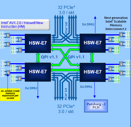
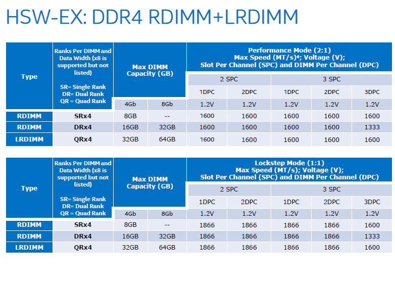
Debuting alongside the Xeon E7 v3 is the new "Jordan Creek 2" buffer chip, which offers support for DDR4 LR-DIMMs or buffered RDIMMs. However if necessary it is still possible to use the original "Jordan Creek" buffer chips with DDR3, giving the Xeon E7 v3 the ability to be used with either DDR3 or DDR4. Meanwhile just like its predecessor, the Jordan Creek 2 buffers can either running in lockstep (1:1) or in performance mode (2:1). If you want more details, read our review of the Xeon E7 v2 or Intel's own comparison.

To sum it up, in lockstep mode (1:1):
- The Scalable Memory Buffer (SMB) is working at the same speed as the RAM, max. 1866 MT/s.
- Offers higher availability as the memory subsystem can recover from two sequential RAM failures
- Has lower bandwidth as the SMB is running at max. 1866 MT/s
- ...but also lower energy for the same reason (about 7W instead of 9W).
In performance mode (2:1):
- You get higher bandwidth as the SMB is running at 3200 MT/s (Xeon E7 v2: 2667 MT/s), twice the speed of the memory channels. The SMB combines two memory channels of DDR-4 1600.
- Higher energy consumption as the SMB is running at full speed (9W TDP, 2.5 W idle)
- The memory subsystem can recover from one device/chip failure as the data can be reconstructed in the spare chip thanks to the CRC chip.
This is a firmware option, so you chose once whether being able to lose 2 DRAM chips is worth the bandwidth hit.
Xeon E7 vs E5
The different platform/system architecture is the way that the Xeon E7 differentiates itself from the Xeon E5, all the while both chips have what is essentially the same die. Besides being able to use 4 and 8 socket configurations, the E7 supports much more memory. Each socket connects via Scalable Memory Interconnect 2 (SMI2) to four "Jordan Creek2" memory controllers.
 Jordan Creek 2 memory buffers under the black heatsinks with 6 DIMM slots
Each of these memory buffers supports 6 DIMM slots. Multiply four sockets with four memory buffers and six dimm slots and you get a total of 96 DIMM slots. With 64 GB LR-DIMMs (see our tests of Samsung/IDT based LRDIMMs here) in those 96 DIMM slots, you get an ultra expensive server with no less than 6 TB RAM. That is why these system are natural hosts for in-memory databases such as SAP HANA and Microsoft's Hekaton.
There is more of course. Chances are uncomfortably high that with 48 Trillion memory cells that one of those will go bad, so you want some excellent reliability features to counter that. Memory mirroring is nothing new, but the Xeon E7 v3 allows you to mirror only the critical part of your memory instead of simply dividing capacity by 2. Also new is "multiple rank sparing", which provides dynamic failover of up to four ranks of memory per memory channel. In other words, not can the system shrug off a single chip failure, but even a complete DIMM failure won't be enough to take the system down either.


146 Comments
View All Comments
PowerTrumps - Saturday, May 9, 2015 - link
I'm sure the author will update the article unless this was a Intel cheerleading piece.name99 - Friday, May 8, 2015 - link
The thing is called E7-8890. Not E7-5890?WTF Intel? Is your marketing team populated by utter idiots? Exactly what value is there in not following the same damn numbering scheme that your product line has followed for the past eight years or so?
Something like that makes the chip look like there's a whole lot of "but this one goes up to 11" thinking going on at Intel...
name99 - Friday, May 8, 2015 - link
OK, I get it. The first number indicates the number of glueless chips, not the micro-architecture generation. Instead we do that (apparently) with a v2 or v3 suffix.I still claim this is totally idiotic. Far more sensible would be to use the same scheme as the other Intel processors, and use a suffix like S2, S4, S8 to show the glueless SMP capabilities.
ZeDestructor - Friday, May 8, 2015 - link
They've been using this convention since Westmere-EX actually, at which point they ditched their old convention of a prefix letter for power tier, followed by one digit for performance/scalability tier, followed by another digit for generation then the rest for individual models. Now we have 2xxx for dual socket, 4xxx for quad socket and 8xxx for 8+ sockets, and E3/E5/E7 for the scalability tier. I'm fine with either, though I have a slight preference for the current naming scheme because the generation is no longer mixed into the main model number.Morawka - Saturday, May 9, 2015 - link
man the power 8 is a beefy cpu... all that cache, you'd think it would walk all over intel.. but intel's superior cpu design winsPowerTrumps - Saturday, May 9, 2015 - link
please explaintsk2k - Saturday, May 9, 2015 - link
Where are the gaming benchmarks?JohanAnandtech - Saturday, May 9, 2015 - link
Is there still a game with software rendering? :-)Gigaplex - Sunday, May 10, 2015 - link
Llvmpipe on Linux gives a capable (feature wise) OpenGL implementation on the CPU.Klimax - Saturday, May 9, 2015 - link
Don't see POWER getting anywhere with that kind of TDP. There will be dearth of datacenters and other hosting locations retooling for such thing. And I suspect not many will even then take it as cooling and power costs will be damn too high.Problem is, IBM can't go lower with TDP as architecture features enabling such performance are directly responsible for such TDP. (Just L1 consumes 2W to keep few cycles latency at high frequency)