The Google Nexus 9 Review
by Joshua Ho & Ryan Smith on February 4, 2015 8:00 AM EST- Posted in
- Tablets
- HTC
- Project Denver
- Android
- Mobile
- NVIDIA
- Nexus 9
- Lollipop
- Android 5.0
GPU Performance
While Denver is new, the Kepler GPU in the Tegra K1 is mostly a known quantity by now. In the Nexus 9, the GPU is still a single SMX clocked to 852 MHz. In order to verify performance, we turn to our standard test suite. For the most part, our GPU-bound tests are meant to represent gaming performance although tests like 3DMark can have CPU-bound aspects while GFXBench tends towards being a pure GPU test.
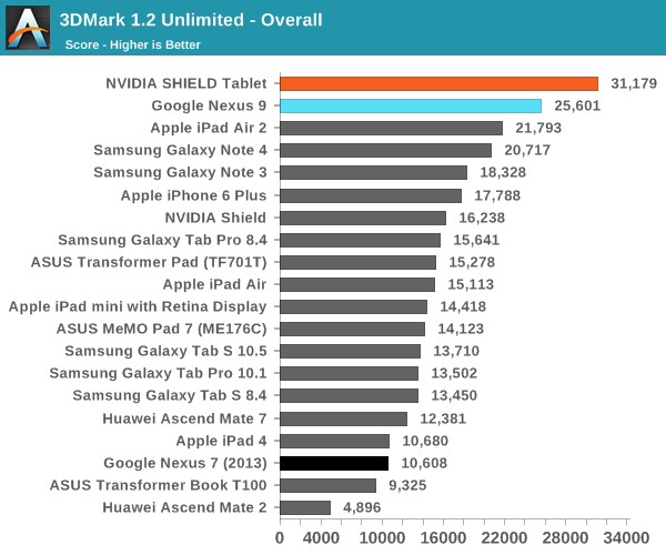
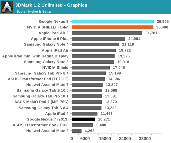
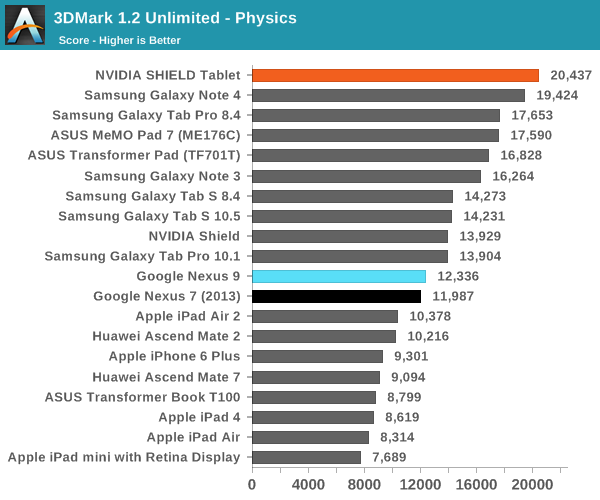
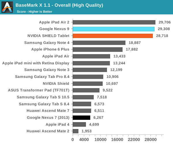
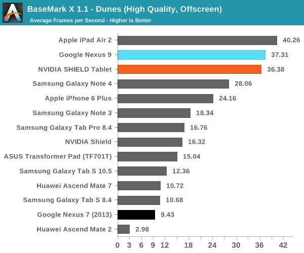
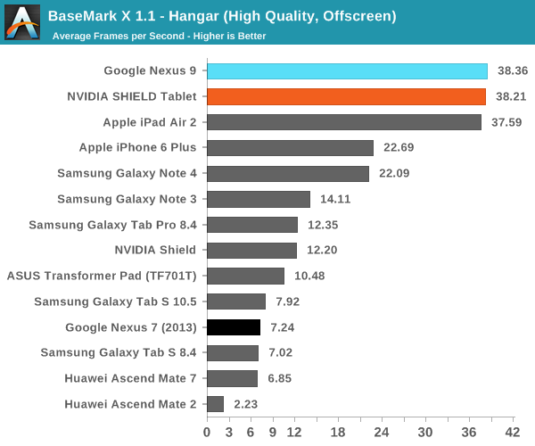
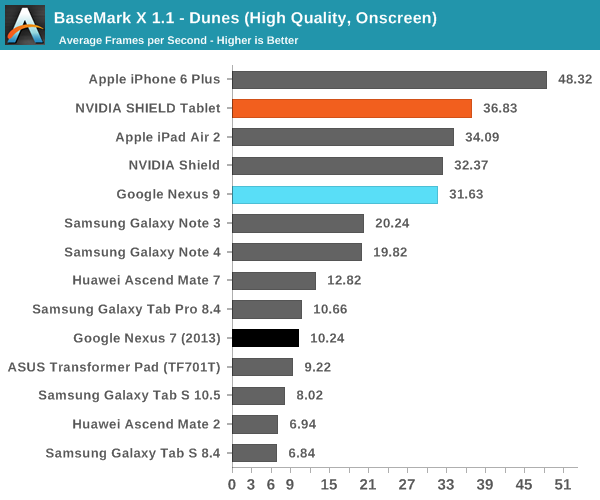
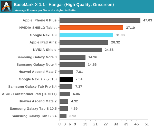
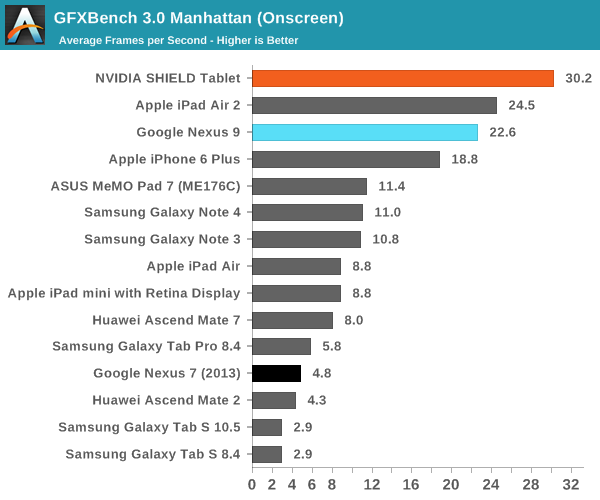
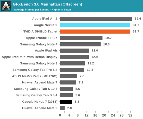
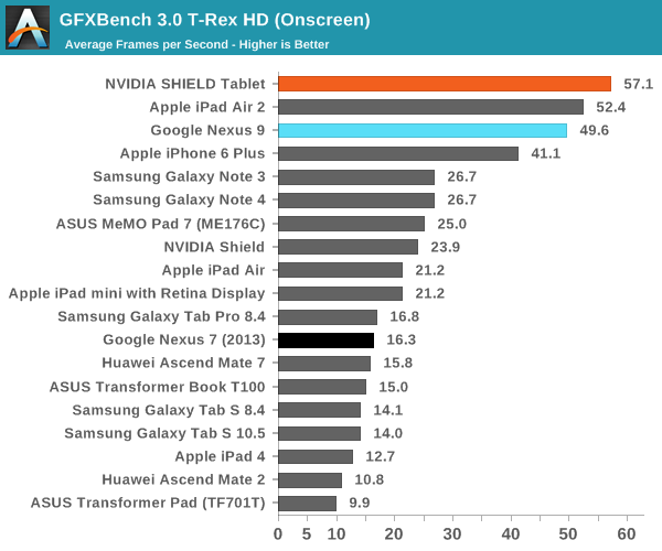
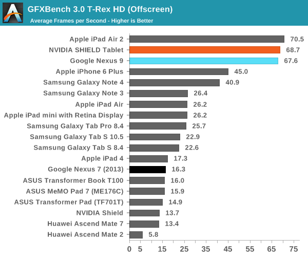
The Nexus 9's GPU has effectively identical performance to what we saw in the SHIELD Tablet, which means that the Nexus 9 should be able to support a broad range of games without performance issues. There is a bit of a noticeable performance delta when comparing on-screen performance, but this is simply due to the higher resolution of the Nexus 9's display. The one notable exception is the 3DMark physics test, which seems to scale with core count quite well, and that causes Denver to fall slightly short of the quad A15 configuration.
NAND Performance
While storage performance can often be secondary to a smooth user experience, poor storage performance is extremely painful. This is similar to RAM, where the difference between 2 and 3 GB is generally academic, while the difference between 512MB and 1 GB is enormous. While there have been some issues with Androbench with the move to Android 5.0, it seems that the timer issues have since been resolved, so it's possible to resume using the results from Androbench to get a rough idea of NAND performance.
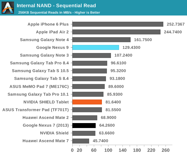
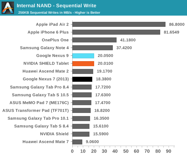
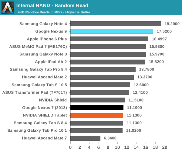
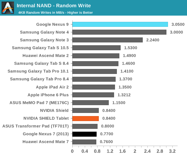
Here the Nexus 9 doesn't suffer nearly as much from full disk encryption that is forcibly enabled on the device; performance is noticeably higher than what we see in the Nexus 6. This seems to lend some credence to the theory that CPUs with ARM v8 ISA would be better suited to handling the need to encrypt and decrypt storage in real time. I tested the Nexus 9 with a custom kernel without full disk encryption to see how Androbench scores might change, but this didn't have a noticeable impact which seems to back this theory, although I'm still not confident that FDE is a good idea to enforce across all new devices.
The NAND itself, a Samsung eMMC package designated by the name BWBC3R, seems to be quite performant outside of pure sequential access, which seems to suggest that HTC hasn't skimped out in this area at all, and the use of F2FS is responsible for some of the best random I/O scores in any mobile devices we've tested thus far.


169 Comments
View All Comments
lucam - Thursday, February 5, 2015 - link
Next time you will write the article for Anand.tuxRoller - Thursday, February 5, 2015 - link
Just tested on my N7 2013. Results were far higher than shown in the chart.SR:64.2->76.1
SW:18.4->30.1
RR:11.2->13.4
RW:0.7->3.1
mpokwsths - Thursday, February 5, 2015 - link
Well, your results are far far more improved than 10% Andrei says.3 devices by 2 different users, all showed vast improvements (10-500%).
Only they refuse to acknowledge it.
Who knows, it seems Anandtech guys are on Apple's payroll...
eiriklf - Thursday, February 5, 2015 - link
Just wanted to note that on the NAND performance front, I believe the android devices which beat the nexus 9 in sequential speed use emmc 5.0 while the nexus uses a high quality emmc 4.5. I think this is because the tegra K1 SoC does not support emmc 5.0.tviceman - Wednesday, February 4, 2015 - link
Better late than never, although being this late is indeed a big letdown.Onto the hardware, looks like Denver is an interesting first custom SoC from Nvidia. Solid in some respects, lacking in others. I think it's a solid building block from which to work on and improve. I hope Nvidia continues the custom ARM core path and gets more design wins (if warranted) moving forward.
kepstin - Wednesday, February 4, 2015 - link
The Denver chip design is pretty interesting, but it reminds me very strongly of another mobile-targeted chip that didn't do well in the marketplace; the Transmeta Crusoe.Both are VLIW designs with in-order execution, both rely on software code translation that runs on the CPU itself. Both even used a partitioned section of system ram as a translated ops cache.
The most significant difference that I see between them is the addition of a native ARM decoder to the Denver CPU; the Crusoe didn't have a native X86 decoder and relied on the dynamic translation for all code that it executed.
I had a Crusoe for a while in a Sony Vaio; it was used in some of the very small/lightweight ultraportable laptops by Japanese manufacturers for a while.
phoenix_rizzen - Wednesday, February 4, 2015 - link
Didn't a large group of Transmeta devs get hired by Nvidia?ABR - Thursday, February 5, 2015 - link
Crusoe lost because Transmeta woke the sleeping giant Intel to the value of low-power, and then a group of 100 people couldn't keep up the resulting engineering race. The x86 world would be a pretty different place today if that hadn't occurred. But I'd say the jury is still out on the overall capability of the VLIW + morphing approach.frenchy_2001 - Thursday, February 5, 2015 - link
I would second that. A quick search returned a licensing agreement where nvidia licensed Transmeta's technology.This could be a good part of Denver.
About in order execution, the biggest experiment was from intel: itanium.
kgh00007 - Wednesday, February 4, 2015 - link
It's 3 months late, the nexus 9 was released on the 3rd of November!!No excuses, but it's just too late to help people make an informed decision!! Just like dog years, one year for a tablet is like 7 technology(dog) years!!