The iPhone 6 Review
by Joshua Ho, Brandon Chester, Chris Heinonen & Ryan Smith on September 30, 2014 8:01 AM EST- Posted in
- Smartphones
- Apple
- Mobile
- iPhone 6
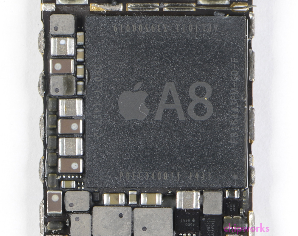
A8: Apple’s First 20nm SoC
As has been customary for every iPhone launch since the company began publicly naming their SoCs, Apple has once again rolled out a new SoC for their latest line of phones. With the launch of the iPhone 6 series Apple is now up to their eight generation SoC, the appropriately named A8.
After a period of rapid change with the A6 and A7 SoCs – which introduced Apple’s first custom CPU design (Swift) and the first ARMv8 AArch64 design (Cyclone) respectively – A8 is a more structured and straightforward evolution of Apple’s SoC designs. Which is not to say that Apple hasn’t been busy tweaking their designs to extract ever-improved performance and power efficiency, as we’ll see, but our examination of A8 has not uncovered the same kind of radical changes that defined A6 and A7.
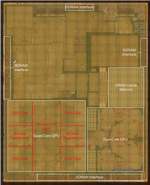
The heart and soul of A8 is as always the CPU and GPU. We’ll be taking a look at each of these individually in a moment, but from a high level both of these are evolutions of their predecessors found in A7. Apple’s GPU of choice remains Imagination’s PowerVR, having upgraded from the Series6 based G6430 to Imagination’s newer GX6450 design. Meanwhile Apple continues to develop their own CPUs and A8 packs their latest design, which is an enhanced version of the Cyclone core first introduced in A7.
Stepping away from the GPU and CPU for the moment, the biggest change about A8 is that it’s smaller. As discovered by Chipworks, A8 is being fabricated on TSMC’s new 20nm process, making the iPhone 6 among the first smartphones to be shipped with a 20nm SoC.
This move to 20nm is not unexpected, but nonetheless it is considerable for a couple of reasons. The first is that this means Apple has moved production over to TSMC’s 20nm HKMG Planar process, making this the first time an Apple SoC has been manufactured anywhere but a Samsung fab. There are numerous possible reasons for this – and not every reason needs to be technical – but from a process development standpoint it’s important to note that over the last few generations TSMC has been the leader among contract foundries, being the first to get new processes up and running for volume production.
| Apple A8 vs A7 SoCs | ||||
| Apple A8 (2014) | Apple A7 (2013) | |||
| Manufacturing Process | TSMC 20nm HKMG | Samsung 28nm HKMG | ||
| Die Size | 89mm2 | 102mm2 | ||
| Transistor Count | ~2B | "Over 1B" | ||
| CPU | 2 x Apple Enhanced Cyclone ARMv8 64-bit cores |
2 x Apple Cyclone ARMv8 64-bit cores |
||
| GPU | IMG PowerVR GX6450 | IMG PowerVR G6430 | ||
This move is also quite considerable because it means for the first time Apple is manufacturing their SoCs on a bleeding edge manufacturing process. Prior to this Apple has been slow to utilize new manufacturing processes, only finally utilizing a 28nm process in late 2013 for A7 over a year after 28nm first became available. The fact that we are seeing a 20nm SoC from Apple at a time when almost everyone else is still on 28nm indicates just how much the market has shifted over the last few years, and how Apple’s SoC development is now synchronized with the very edge of semiconductor fabrication technology.
Finally, the switch to 20nm is interesting because after the last couple of generations being so-called “half node” jumps – 45nm to 40nm to 32nm to 28nm – the jump from 28nm to 20nm is a full node jump (note that Apple didn't ever use 40nm, however). This means we are seeing a larger increase in transistor density than in the previous generations, and ideally a larger decrease in power consumption as well.
In practice TSMC’s 20nm process is going to be a mixed bag; it can offer 30% higher speeds, 1.9x the density, or 25% less power consumption than their 28nm process, but not all three at once. In particular power consumption and speeds will be directly opposed, so any use of higher clock speeds will eat into power consumption improvements. This of course gets murkier once we’re comparing TSMC to Samsung, but the principle of clock speed/power tradeoffs remains the same regardless.
Not accounting for minor differences between TSMC and Samsung, in an ideal case Apple is looking at 51% area scaling (the same design on 20nm can be no smaller than 51% of the die area at 28nm). In reality, nothing ever scales perfectly so the density gains will depend on the kind of I/C being laid down (logic, SRAM, etc.). For the complete chip a 60-70% scaling factor is going to be a better approximation, which for Apple means they’ve picked up a lot room to spend on new functionality and reducing their overall die size.
| Apple SoC Evolution | |||||
| CPU Perf | GPU Perf | Die Size | Transistors | Process | |
| A5 | ~13x | ~20x | 122m2 | <1B | 45nm |
| A6 | ~26x | ~34x | 97mm2 | <1B | 32nm |
| A7 | 40x | 56x | 102mm2 | >1B | 28nm |
| A8 | 50x | 84x | 89mm2 | ~2B | 20nm |
Meanwhile once again this year Apple opened up on die size and transistor counts. A8 weighs in at around 2 billion transistors, as opposed to the “over 1 billion” transistors found on A7. We also have the die size for A8 – 89mm2 – which is some 13% smaller than A7’s 102mm2 die. This makes it clear that Apple has chosen to split their transistor density improvements between adding features/performance and reducing their size, rather than going all-in on either direction.
In the case of using a bleeding edge node this is generally a good call, as Apple and TSMC will need to deal with the fact that chip yields at 20nm will not be as good as they are on the highly mature 28nm process. With lower chip yields, a smaller die will offset some of those yield losses by reducing the number of manufacturing flaws any given die touches, improving the overall yield.
A8 With POP RAM Removed
Moving on, looking at A8 we can see that Apple’s memory subsystem design has not significantly changed from A7. Once again Apple has placed an SRAM cache on the chip to service both the CPU and the GPU. Based on an examination of the die and of latency numbers, this L3 SRAM cache remains unchanged from A7 at 4MB. Meanwhile we also find a series of SDRAM interfaces which drive the A8’s package-on-package (POP) based main memory. Based on teardowns from iFixit, Apple is using 1GB of LPDDR3-1600, the same speed grade of LPDDR3 and capacity that they used for the iPhone 5s. iFixit has found both Hynix and Elpida memory in their phones, so Apple is once again using multiple sources for their RAM.
When we start poking at memory bandwidth we find that memory bandwidths are consistently higher than on A7, but only ever so slightly. This points to Apple having worked out further optimizations to make better use of the memory bandwidth they have available, since as we’ve previously determined they’re still using LPDDR3-1600 speeds.
| Geekbench 3 Memory Bandwidth Comparison (1 thread) | ||||||
| Stream Copy | Stream Scale | Stream Add | Stream Triad | |||
| Apple A8 1.4GHz | 9.08 GB/s | 5.37 GB/s | 5.76 GB/s | 5.78 GB/s | ||
| Apple A7 1.3GHz | 8.34 GB/s | 5.21 GB/s | 5.67 GB/s | 5.69 GB/s | ||
| A8 Advantage | 9% | 3% | 2% | 2% | ||
The Stream Copy score ends up being the biggest gain at 9%. Otherwise the rest of the benchmarks only show 2-3% memory bandwidth increases.
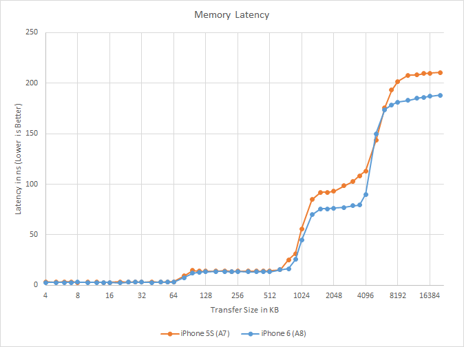
More interesting is memory latency, which shows some unexpected improvements once we get out of the L1 and L2 caches. At both the 1MB – 4MB region of the SRAM and 6MB+ region of main memory, memory latency is consistently lower on A8 versus A7. In both cases we’re looking at latencies about 20ns faster than A7. This identical 20ns gain tells us that that Apple is still doing main memory lookups after the L3 lookup fails, and this in turn means the 20ns gain we’re seeing is due to L3 cache optimizations. We have a couple of ideas for how Apple could have improved L3 latency by nearly 20% like this, but at this time with Apple staying quiet on their architecture like usual, it’s not apparent which of these ideas are the correct ones.
Turning our eyes back to A8 one final time, we find that while a lot of die space is occupied by the CPU, GPU, and SRAM (as we’d expect), there is also quite a bit of space occupied by other blocks Apple has integrated into their design. Without already knowing what you’re looking for these blocks are difficult to identify, but even without being able to do this we have a reasonable idea of what blocks Apple has integrated. Among these we’ll find audio controllers, USB controllers, video encoders/decoders, flash memory controllers, the camera ISP, and of course all kinds of interconnect.
All of these blocks are fixed function hardware (or at best, limited flexibility DSPs), which are equally important to not only the A8’s functionality but power efficiency. By assigning tasks to dedicated hardware Apple does spend some die space on that hardware, but in return these blocks are more efficient than doing those tasks entirely in software. Hence Apple (and SoC designers in general) have a strong incentive to offload as much work as possible to keep power consumption in check. This move towards more fixed function hardware is part of a general “wheel of reincarnation” cycle that has been a constant in processor design over the years, which sees a continuous shift between fixed function and programmable hardware. SoCs, for the most part, are still going towards fixed function hardware, and this should continue for a while yet.
In any case, while we can’t identify individual blocks on A8 we do know that Apple has added a few features to A8 that are present in some form or another among these blocks. New to A8 is some mix of H.265 (HEVC) hardware, which would be necessary to enable the FaceTime over H.265 functionality that is being introduced on the iPhone 6. Apple’s “desktop class scaler” that is used for handling non-native resolution applications and for down-sampling the internal rendering resolution of the iPhone 6 Plus would also be present here.


531 Comments
View All Comments
Toss3 - Thursday, October 9, 2014 - link
The browser benchmarks would make more sense if they used the stock browser on all the devices, not just on the iPhone to make it look good. The Note 4 for instance is scoring around 350ms with its own browser, while on Chrome it is only seeing 800ms. The results should also be in a separate "Web-browsing performance" section instead of the CPU performance one.thackr - Thursday, October 9, 2014 - link
Does anyone else see the green dot lens flare shown here on their iPhone 6? http://www.alternapop.com/2014/10/02/iphone-6-lens...The0ne - Friday, October 10, 2014 - link
"At this point, it’s not really possible to revolutionize the smartphone..."Stopped when I got here. I don't usually cuss but you have got to be shtting me for making such a statement. In your effort to try to write a unbiased review you are already stating that for whatever the reasons the phone may lack it is because nothing can be improve so it's a great phone. I officially hate all your Apple reviews now. This is sickening for any professional engineer to digest.
JC86 - Friday, October 10, 2014 - link
@TheOne: Engineers are constantly tweaking and refining the software and hardware for a better UX and that refinement is great but the bottom line is the modern smartphone as we know it have not had any revolutionary advancements in years. It's a mature product category, plain and simple.tralalalalalala40 - Friday, October 10, 2014 - link
So you're one of those that thinks cars are changing massively every year. "THE BRAND NEW REVOLUTION IS HERE FOR A LIMITED TIME"sgmuser - Sunday, October 12, 2014 - link
"and how Apple’s SoC development is now synchronized with the very edge of semiconductor fabrication technology." You are not kidding right! :-) Comparing Intel's 14nm chips, I still believe Mobile phone SoCs are not coping up with the latest tech. m2c. Samsung (with Exynos) atleast jumped a bit...comparing QC SD or Apple Ax series.Pandian - Sunday, October 12, 2014 - link
Actually, Intel is not in making chips, 14nm or 20nm, for cell phones at large! Such a big company with capacity to supply designer boards to any manufacturer in the handheld 3inch or 12 inch device - and still staying away!Pandian - Sunday, October 12, 2014 - link
Compare these - Apple, etc. and All Pharma! 2-5% on actual R&D by pharmaceutical companies, (esp., the ones pricing cancer and Hepatitis C drugs) and about 95 % on marketing (read bribing the Medical industry - that includes "respectable life-saving Doctors") - vs 20-50% profit by tech companies (Apple, Samsung, Lenovo, HP, etc.) on products made from R&D from this decade! Without the slave labor of China and such countries, even that profit is not possible! Today's pyramids and Taj Mahals!Drugs: Most of these drugs were "discovered" decades ago in govt. research facilities - somehow, they are private intellectual properties today! Even anti-helminths (drugs for cattle parasites) costing ~$1-10 for 1000 pills, suddenly cost up to thousands of dollars each pill, because their anti-cancer capacities were "discovered" as side-effects! Even aspirin, made in third world countries and sold here, costs about ten times from a decade or so ago, due to price fixing!
Your life or $200,000 - pay-up or die, if you have cancer or Hepatitis C.
The target is larger with cellphones and computers - hence the bigger market value of the companies!
Even within the tech industry, the profit of $200-300 for each device is paid once every three years or so - the cost of gasoline for a car is more than that in 2-3 months! The actual leaches that cost the consumer are the cell and cable/satellite companies - thousands of dollars a family in a two year contract! USA still charges the highest fee for cell plans, voice, text and data - taking a bite at each end of the link, i.e., the caller and the recipient!
And, we whine more about the cost of these hand-held toys - that is the purpose and use of most of these "smart" devices! Truly important communication via voice, or the equivalent of the Morse code or ham-radio, is so small - not worth taking care of while driving a 4000+lb missile at 55 to 80 mph!
Both Apple and Samsung will take a dive in the next 12 months
A millionaire on CNBC talked about not being eligible for a phone upgrade for another year - and therefore not having hands-on experience with the recently released phones, Apple, HTC, etc.! That is how you stay rich!
The post seems irrelevant! No! The basic premise of most of the posts here are about MONEY!
xmen77 - Monday, October 13, 2014 - link
There can not be "ideal 6500k" if the other LCD in this all badalso
phonearena.com/reviews/Screen-comparison-iPhone-6-vs-Galaxy-S5-vs-G3-vs-One-M8-vs-iPhone-5s_id3810
this is "ideal 6500k"?
thrasher32 - Tuesday, October 14, 2014 - link
Yeah I'm just gonna say it: Apple is the Bose of mobile electronics, only those who don't know any better buy that junk. Hey it's your money feel free to waste as much as you like.