The NVIDIA GeForce GTX 980 Review: Maxwell Mark 2
by Ryan Smith on September 18, 2014 10:30 PM ESTMaxwell 2 Architecture: Introducing GM204
Now that we’ve had a chance to recap Maxwell 1 and what went into that architecture, let’s talk about the first of the second generation Maxwell GPUs, the GM204.
GM204 may be a second generation Maxwell part, but it is without question still a Maxwell part. Maxwell has learned some new tricks that we are going to cover here, but functionally speaking you can consider GM204 to be a bigger version of GM107, taking more SMMs and more ROP/memory partitions and using them to build a bigger, more powerful GPU.
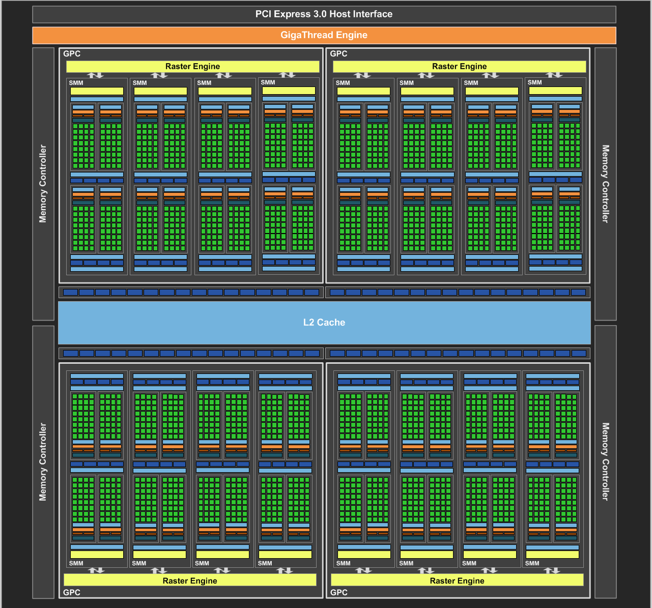
With GM107 being built from 5 SMMs, GM204 is a bit more than a triple GM107. Altogether NVIDIA is building GM204 out of 16 SMMs, this time divided up into 4 GPCs instead of GM107’s single GPC. This is bound to 64 ROPs and 4 64bit memory controllers, which is a 4x increase in the number of ROPs compared to GM107, and a 2x increase in the memory bus size.
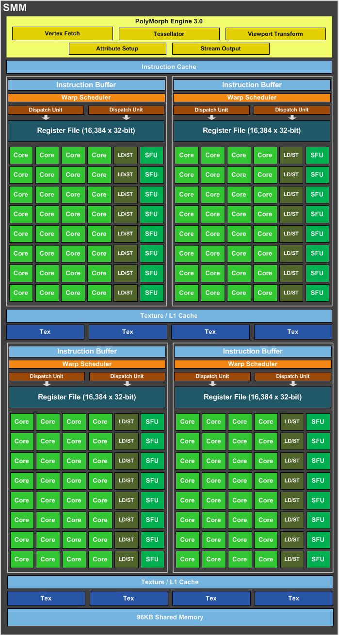
Drilling down to the SMMs for a second, there are a couple of small changes that need to be noted. Organizationally the GM204 SMM is identical to the GM107 SMM, however GM204 gets 96KB of shared memory versus 64KB on GM107. Separate from the combined L1/texture cache, this shared memory services a pair of SMMs and their associated texture units to further reduce the need to go to L2 cache or beyond.
The Polymorph Engines have also been updated. There are not any major performance differences with the 3.0 engines, but they are responsible for implementing some of the new functionality we’ll reference later.
Other than this, GM204’s SMM is identical to the GM107 SMM. This includes the use of 4 shared texture units per 2 SMMs, leading to a 16:1 compute-to-texture ratio, and a 512Kb register file for each SMM.
Compared to GK104 of course this is a more remarkable change. Compared to its immediate predecessor, GM204 sees significant differences in both the layout of the SMM and of the resulting chip, which means that even before accounting for feature differences we can’t just start counting functional units and directly comparing GM204 to GK104. GM204 is overall a more efficient chip, and although it possesses just 33% more CUDA cores than GK104 its performance advantage is much greater, on the order of 50% or more, highlighting the fact that NVIDIA is getting more work out of their CUDA cores than ever before. Altogether, NVIDIA tells us that on average they’re getting 40% more performance per core, which is one of the reasons why GTX 980 can beat even the full GK110 based GTX 780 Ti, with its 2880 CUDA cores.
Compute hardware aside, fleshing out GM204 is of course the ROP/memory partitions. Although the constituent hardware hasn’t changed much – we’re still looking at 7GHz GDDR5 memory controllers and the same pixel throughput per ROP – GM204 is very atypical for its configuration of these parts.
Until now, high-end NVIDIA designs have used an 8:1 ratio; 8 ROPs (or rather ROPs that process 8 pixels per clock) paired up with each 64bit memory controller. This gave GK104 32 ROPs, GK110 48 ROPs, and GM107 16 ROPs. However beginning with GM204 NVIDIA has increased the ROP-to-memory ratio and as a result has doubled their total ROP count compared to GK104. GM204 features a 16:1 ratio, giving us our first NVIDIA GPU with 64 ROPs.
Now the subject of ROPs is always a dicey one because of the nature of pixel operations. Unlike compute hardware, which can be scaled up rather effectively with more complex workloads and better caching methods, the same is not true for ROPs. ROPs are the ultimate memory bandwidth burner. They are paired with memory controllers specifically because the work they do – the Z testing, the pixel blending, the anti-aliasing – devours immense amounts of bandwidth. As a result, even if you are bottlenecked by ROP performance increasing the ROP count won’t necessarily be performance effective if those ROPs are going to be bandwidth starved.
| NVIDIA ROP To Memory Controller Ratios | |||||
| GPU | ROP:MC Ratio | Total ROPs | |||
| Maxwell (GM204) | 16:1 | 64 | |||
| Maxwell (GM107) | 8:1 | 16 | |||
| Kepler (GK110) | 8:1 | 48 | |||
| Fermi (GF110) | 8:1 | 48 | |||
| GT200 | 4:1 | 32 | |||
The last time NVIDIA increased their ROP ratio was for Fermi, when it went from 4:1 to 8:1. This was largely fueled by the introduction of GDDR5, whose higher data rates provided the bandwidth necessary to feed the greater number of ROPs. Since then GDDR5 clockspeeds have increased a bit for NVIDIA, from 4GHz to 7GHz, but so have ROP clockspeeds as well, meaning there hasn’t been a significant change in the ability for NVIDIA’s memory controllers to feed their ROPs since Fermi.
Consequently making the jump to a 16:1 means that change would need to happen somewhere else. This has led to NVIDIA approaching the problem from the other direction: instead of increasing the available memory bandwidth, what can they do to reduce it?
Color Compression
The solution, and really the key to making a 16:1 ROP ratio feasible, is the latest generation of NVIDIA’s delta color compression technology. Color compression in and of itself is not new technology, but over successive hardware generations NVIDIA has continued to iterate on it, and as such has continued to increase the amount of data they can compress.
NVIDIA first introduced color compression on the GeForce FX series, where it could compress data at up to a 4:1 ratio. The actual compressibility of any frame would in turn depend on the contents of the frame. At a most basic level NVIDIA would break down a frame into regions and then attempt to find smaller portions of redundant data to compress. Anti-aliasing was especially favorable here, as anti-aliasing samples would frequently all be of a fully covered triangle, resulting in all pixels being identical. In the case of regular color compression the key is finding whole regions of identical colors, at which point you could potentially compress them down by as much as 8:1.
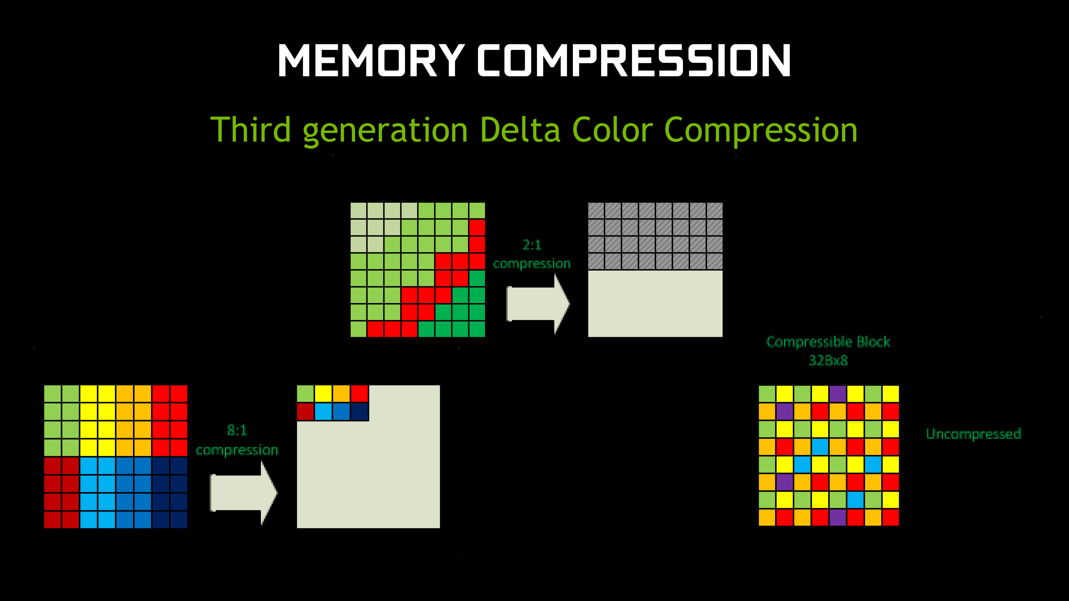
More recently, in Fermi NVIDIA introduced delta color compression, which is designed to take color compression beyond simple regions containing identical pixels. Delta color compression is essentially focused on pattern compression instead of region compression, compressing based on the differences (delta) between pixels rather than how they’re identical; if you can describe how the pixels will differ from one-another, then you can save space describing the delta instead of the individual pixel. Delta color compression works off of the same blocks and essentially applies different delta patterns to them, attempting to find the best pattern for the block.
Delta compression is by its nature less efficient than whole color compression, topping out at just 2:1 compared to 8:1 for the latter. However a 2:1 ratio is still potentially a 50% reduction in data size, which is far better than letting the data go uncompressed. At 4x2 32bit pixels per region, this would mean reducing a region from 32 bytes to 16 bytes.
NVIDIA’s 3rd generation of color compression then is the latest iteration on this technology. The fundamentals between the various generations of delta color compression have not changed, but with each iteration NVIDIA has gained the ability to apply more and more patterns to the blocks to find better matches. 3rd generation delta color compression offers the most patterns yet, and the most opportunity to compress pixel blocks.
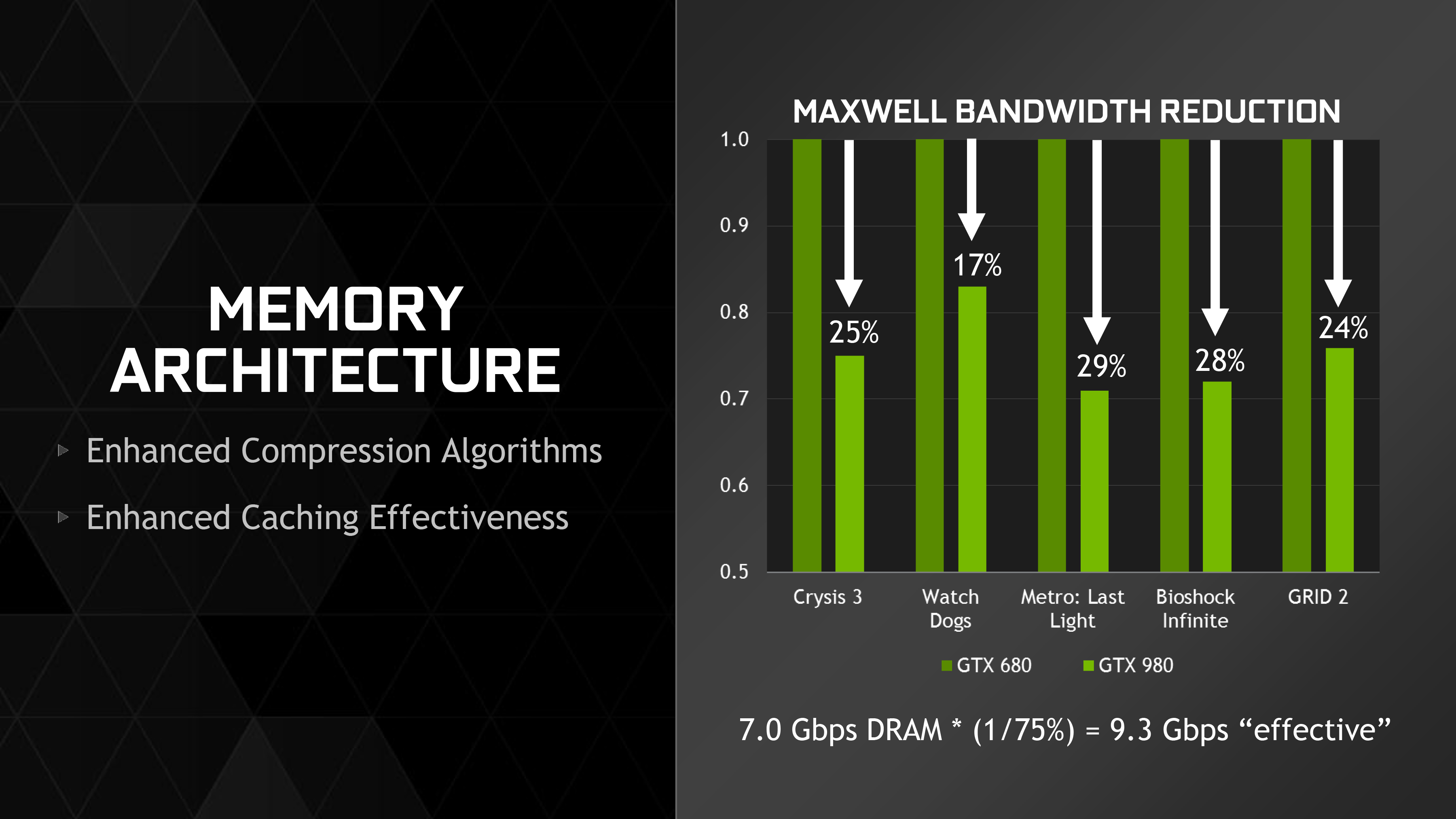
The importance of color compression cannot be understated. The impact of 3rd generation delta color compression is enough to reduce NVIDIA’s bandwidth requirements by 25% over Kepler, and again this comes just from having more delta patterns to choose from. In fact color compression is so important that NVIDIA will actually spend multiple cycles trying different compression ratios, simply because the memory bandwidth is more important than the computational time.
Getting back to our ROPs then, it’s the introduction of 3rd generation color compression, which alongside the larger 2MB L2 cache, makes a 16:1 ROP ratio on GM204 viable. Being able to feed 64 ROPs in turn helps NVIDIA’s overall performance, especially at higher resolutions. With 4K monitors taking off NVIDIA needs to be able to offer competitive performance at those resolutions, and while doubling the number of ROPs won’t double NVIDIA’s performance, it none the less is an essential part of being able to scale up performance for the needs of 4K. AMD for their part already went to 64 ROPs on their high-end GPU with Hawaii last year, and while the subject isn’t nearly as simple as just comparing ROP counts, it was one of the factors that resulted in the superior 4K performance scaling we saw from Hawaii cards.
Die Size & Power
Last but certainly not least, now that we’ve had a chance to discuss the architecture of GM204, let’s talk about its physical properties.
One of the problems posed by remaining on the 28nm process is that increasing CUDA core counts will result in larger GPUs. NVIDIA has actually done quite a bit of work on chip density, and as a result the increase in chip size is not going to be as great as the increase in the underlying hardware. Still, GM204 is a more powerful and more complex chip than GK104, and as a result die size and transistor count has gone up.
GM204 ends up weighing in at 5.2 billion transistors, with a die size of 398mm2. This compares to 3.54B transistors and a die size of 294mm2 for GK104, and 7.1B transistors and 551mm2 for GK110. Compared to either Kepler design the overall transistor density is improved, albeit not significantly so.
More important is the fact that GM204 ends up being NVIDIA’s largest xx4 class GPU. xx4 GPUs are typically NVIDIA’s midrange to high-end consumer workhorses, designed first and foremost for graphics and not packing the advanced compute features such as high speed FP64 and ECC memory support that we see in the big x00/x10 GPUs. For cost and overlap reasons NVIDIA’s sweet spot up until now has been around 300-350mm2, with GK104 coming in a hair ahead of the curve. But at just shy of 400mm2, GM204 is encroaching on newer, larger territory.
To some degree this is an inevitable result of remaining on the 28nm process. More performance requires more transistors, and as a result die size was destined to go up. None the less the fact that NVIDIA is fabricating such a large GPU as an xx4 GPU is remarkable. It provides a good example of just how much hardware (in terms of transistors) NVIDIA had to throw in to reach their performance goals. Alternatively, it’s telling that NVIDIA is now going to be able to use a 398mm2 chip as the basis of their high-end consumer video card, as opposed to having to use a 551mm2 chip in the form of GK110.
What’s particularly interesting though is that despite the big die, NVIDIA’s power consumption is exceptionally low. By historical standards GK104 was already a low power GPU for its size, this being the case particularly for GTX 680. GTX 680 was a 195W TDP part with a GPU Boost 1.0 power target of 170W. The GM204 based GTX 980 on the other hand, despite packing in nearly 1.5B more transistors for another 104mm2 of die size, actually consumes less power than said GK104 based card. At 165W TDP NVIDIA’s energy efficiency optimizations are in full effect, and it means NVIDIA consumes surprisingly little power for such a large GPU.
Impressively, all of this comes at the same time that NVIDIA is clocking the GPU at over 1.2GHz. This means we are not looking at a simple case of wide-and-slow, as is often the case for power optimized GPUs (see: SoCs). NVIDIA is clocking GM204 high and hitting it with over 1.2v, and yet it’s still able to maintain a 165W TDP in spite of its large die size. We’ll look at the competitive ramifications of this later, but to keep power consumption so low on such a large GPU really is a feather in NVIDIA’s cap.


274 Comments
View All Comments
garadante - Sunday, September 21, 2014 - link
What might be interesting is doing a comparison of video cards for a specific framerate target to (ideally, perhaps it wouldn't actually work like this?) standardize the CPU usage and thus CPU power usage across greatly differing cards. And then measure the power consumed by each card. In this way, couldn't you get a better example ofgaradante - Sunday, September 21, 2014 - link
Whoops, hit tab twice and it somehow posted my comment. Continued:couldn't you get a better example of the power efficiency for a particular card and then meaningful comparisons between different cards? I see lots of people mentioning how the 980 seems to be drawing far more watts than it's rated TDP (and I'd really like someone credible to come in and state how heat dissipated and energy consumed are related. I swear they're the exact same number as any energy consumed by transistors would, after everything, be released as heat, but many people disagree here in the comments and I'd like a final say). Nvidia can slap whatever TDP they want on it and it can be justified by some marketing mumbo jumbo. Intel uses their SDPs, Nvidia using a 165 watt TDP seems highly suspect. And please, please use a nonreference 290X in your reviews, at least for a comparison standpoint. Hasn't it been proven that having cooling that isn't garbage and runs the GPU closer to high 60s/low 70s can lower power consumption (due to leakage?) something on the order of 20+ watts with the 290X? Yes there's justification in using reference products but lets face it, the only people who buy reference 290s/290Xs were either launch buyers or people who don't know better (there's the blower argument but really, better case exhaust fans and nonreference cooling destroys that argument).
So basically I want to see real, meaningful comparisons of efficiencies for different cards at some specific framerate target to standardize CPU usage. Perhaps even monitoring CPU usage over the course of the test and reporting average, minimum, peak usage? Even using monitoring software to measure CPU power consumption in watts (as I'm fairly sure there are reasonably accurate ways of doing this already, as I know CoreTemp reports it as its probably just voltage*amperage, but correct me if I'm wrong) and reported again average, minimum, peak usage would be handy. It would be nice to see if Maxwell is really twice as energy efficient as GCN1.1 or if it's actually much closer. If it's much closer all these naysayers prophesizing AMD's doom are in for a rude awakening. I wouldn't put it past Nvidia to use marketing language to portray artificially low TDPs.
silverblue - Sunday, September 21, 2014 - link
Apparently, compute tasks push the power usage way up; stick with gaming and it shouldn't.fm123 - Friday, September 26, 2014 - link
Don't confuse TDP with power consumption, they are not the same thing. TDP is for designing the thermal solution to maintain the chip temperature. If there is more headroom in the chip temperature, then the system can operate faster, consuming more power."Intel defines TDP as follows: The upper point of the thermal profile consists of the Thermal Design Power (TDP) and the associated Tcase value. Thermal Design Power (TDP) should be used for processor thermal solution design targets. TDP is not the maximum power that the processor can dissipate. TDP is measured at maximum TCASE"
https://www.google.com/url?sa=t&source=web&...
NeatOman - Sunday, September 21, 2014 - link
I just realized that the GTX 980 has a TDP of 165 watts, my Corsair CX430 watt PSU is almost overkill!, that's nuts. That's even enough room to give the whole system a very good stable overclock. Right now i have a pair of HD 7850's @ stock speed and a FX-8320 @ 4.5Ghz, good thing the Corsair puts out over 430 watts perfectly clean :)Nfarce - Sunday, September 21, 2014 - link
While a good power supply, you are leaving yourself little headroom with 430W. I'm surprised you are getting away with it with two 7850s and not experiencing system crashes.ET - Sunday, September 21, 2014 - link
The 980 is an impressive feat of engineering. Fewer transistors, fewer compute units, less power and better performance... NVIDIA has done a good job here. I hope that AMD has some good improvements of its own under its sleeve.garadante - Sunday, September 21, 2014 - link
One thing to remember is they probably save a -ton- of die area/transistors by giving it only what, 1/32 double precision rate? I wonder how competitive in terms of transistors/area an AMD GPU would be if they gutted double precision compute and went for a narrower, faster memory controller.Farwalker2u - Sunday, September 21, 2014 - link
I am looking forward to your review of the GTX 970 once you have a compatible sample in hand.I would like to see the results of the Folding @Home benchmarks. It seems that this site is the only one that consistently use that benchmark in its reviews.
As a "Folder" I'd like to see any indication that the GTX 970, at a cost of $330 and drawing less watts than a GTX 780; may out produce both the 780 ($420 - $470) and the 780Ti ($600). I will be studying the Folding @ Home: Explicit, Single Precision chart which contains the test results of the GTX 970.
Wolfpup - Monday, September 22, 2014 - link
Wow, this is impressive stuff. 10% more performance from 2/3 the power? That'll be great for desktops, but of course even better for notebooks. Very impressed they could pulll off that kind of leap on the same process!They've already managed to significantly bump up the top end mobile part from GTX 680 -> 880, but within a year or so I bet they can go quite a bit higher still.
Oh well, it was nice having a top of the line mobile GPU for a while LOL
If 28nm hit in 2012 though, doesn't that make 2015 its third year? At least 28nm seems to be a really good process, vs all the issues with 90/65nm, etc., since we're stuck on it so long.
Isn't this Moore's Law hitting the constraints of physical reality though? We're taking longer and longer to get to progressively smaller shrinks in die size, it seems like...
Oh well, 22nm's been great with Intel and 28's been great with everyone else!