The NVIDIA GeForce GTX 980 Review: Maxwell Mark 2
by Ryan Smith on September 18, 2014 10:30 PM ESTOverclocking GTX 980
One of GTX 750 Ti’s more remarkable features was its overclocking headroom. GM107 could overclock so well that upon initial release, NVIDIA did not program in enough overclocking headroom in their drivers to allow for many GTX 750 Ti cards to be overclocked to their true limits. This is a legacy we would be glad to see repeated for GTX 980, and is a legacy we are going to put to the test.
As with NVIDIA’s Kepler cards, NVIDIA’s Maxwell cards are subject to NVIDIA’s stringent power and voltage limitations. Overvolting is limited to NVIDIA’s built in overvoltage function, which isn’t so much a voltage control as it is the ability to unlock 1-2 more boost bins and their associated voltages. Meanwhile TDP controls are limited to whatever value NVIDIA believes is safe for that model card, which can vary depending on its GPU and its power delivery design.
For GTX 980 we have a 125% TDP limit, meanwhile we are able to overvolt by 1 boost bin to 1265MHz, which utilizes a voltage of 1.25v.
| GeForce GTX 980 Overclocking | ||||
| Stock | Overclocked | |||
| Core Clock | 1126MHz | 1377MHz | ||
| Boost Clock | 1216MHz | 1466MHz | ||
| Max Boost Clock | 1265MHz | 1515MHz | ||
| Memory Clock | 7GHz | 7.8GHz | ||
| Max Voltage | 1.25v | 1.25v | ||
GTX 980 does not let us down, and like its lower end Maxwell 1 based counterpart the GTX 980 turns in an overclocking performance just short of absurd. Even without real voltage controls we were able to push another 250MHz (22%) out of our GM204 GPU, resulting in an overclocked base clock of 1377MHz and more amazingly an overclocked maximum boost clock of 1515MHz. That makes this the first NVIDIA card we have tested to surpass both 1.4GHz and 1.5GHz, all in one fell swoop.
This also leaves us wondering just how much farther GM204 could overclock if we were able to truly overvolt it. At 1.25v I’m not sure too much more voltage is good for the GPU in the long term – that’s already quite a bit of voltage for a TSMC 28nm process – but I suspect there is some untapped headroom left in the GPU at higher voltages.
Memory overclocking on the other hand doesn’t end up being quite as extreme, but we’ve known from the start that at 7GHz for the stock memory clock, we were already pushing the limits for GDDR5 and NVIDIA’s memory controllers. Still, we were able to work another 800MHz (11%) out of the memory subsystem, for a final memory clock of 7.8GHz.
Before we go to our full results, in light of GTX 980’s relatively narrow memory bus and NVIDIA’s color compression improvements, we quickly broke apart our core and memory overclock testing in order to test each separately. This is to see which overclock has more effect: the core overclock or the memory overclock. One would presume that the memory overclock is the more important given the narrow memory bus, but as it turns out that is not necessarily the case.
| GeForce GTX 980 Overclocking Performance | |||||
| Core (+22%) | Memroy (+11%) | Combined | |||
| Metro: LL |
+15%
|
+4%
|
+20%
|
||
| CoH2 |
+19%
|
+5%
|
+20%
|
||
| Bioshock |
+9%
|
+4%
|
+15%
|
||
| Battlefield 4 |
+10%
|
+6%
|
+17%
|
||
| Crysis 3 |
+12%
|
+5%
|
+15%
|
||
| TW: Rome 2 |
+16%
|
+7%
|
+20%
|
||
| Thief |
+12%
|
+6%
|
+16%
|
||
While the core overclock is greater overall to begin with, what we’re also seeing is that the performance gains relative to the size of the overclock consistently favor the core overclock to the memory overclock. With a handful of exceptions our 11% memory overclock is netting us less than a 6% increase in performance. Meanwhile our 22% core overclock is netting us a 12% increase or more. This despite the fact that when it comes to core overclocking, the GTX 980 is TDP limited; in many of these games it could clock higher if the TDP budget was large enough to accommodate higher sustained clockspeeds.
Memory overclocking is still effective, and it’s clear that GTX 980 spends some of its time memory bandwidth bottlenecked (otherwise we wouldn’t be seeing even these performance gains), but it’s simply not as effective as core overclocking. And since we have more core headroom than memory headroom in the first place, it’s a double win for core overclocking.
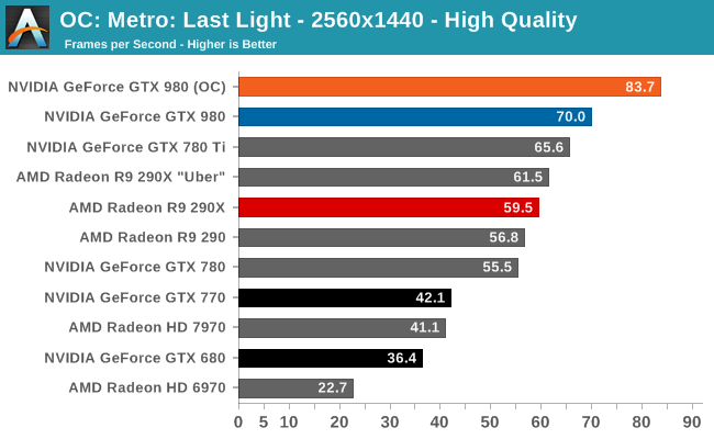
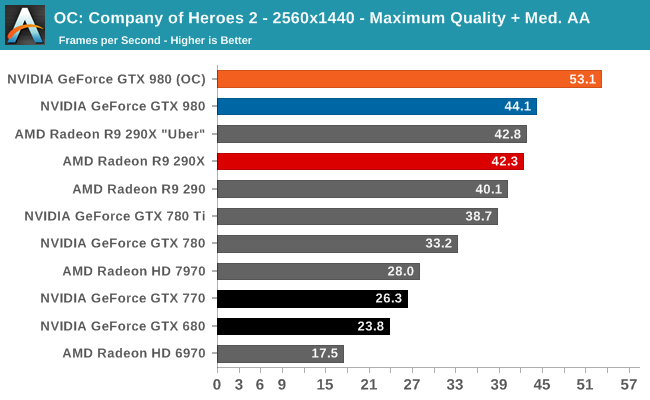
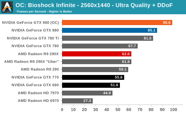
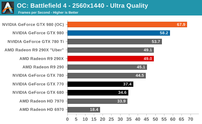
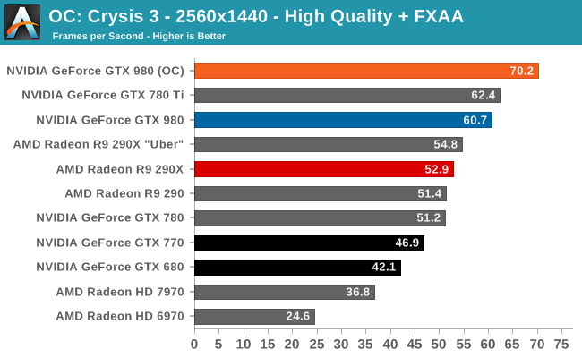
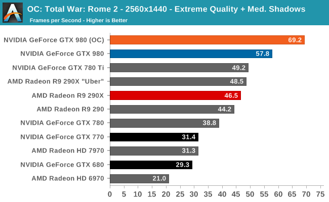
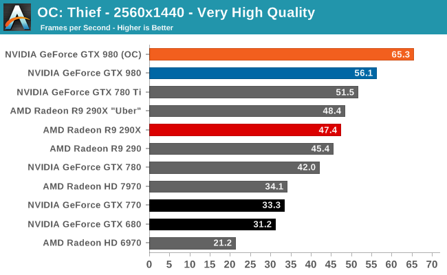
To put it simply, the GTX 980 was already topping the charts. Now with overclocking it’s another 15-20% faster yet. With this overclock factored in the GTX 980 is routinely 2x faster than the GTX 680, if not slightly more.
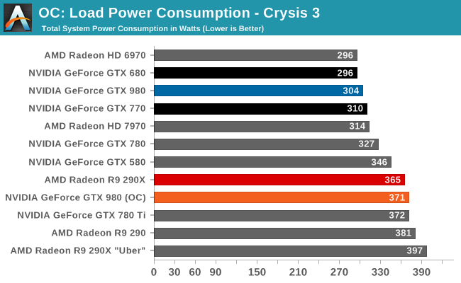
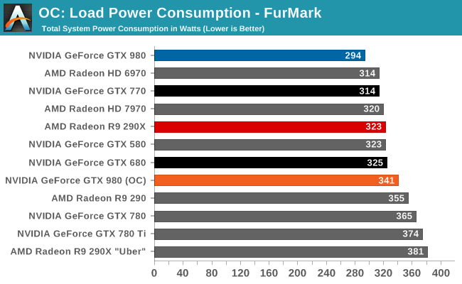
But you do pay for the overclock when it comes to power consumption. NVIDIA allows you to increase the TDP by 25%, and to hit these performance numbers you are going to need every bit of that. So what was once a 165W card is now a 205W card.
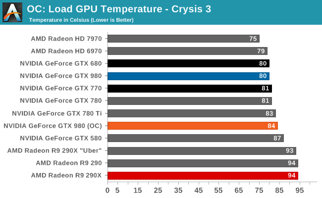
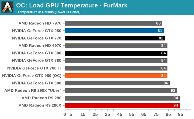
Even though overclocking involves raising the temperature limit to 91C, NVIDIA's fan curve naturally tops out at 84C. So even in the case of overclocking the GTX 980 isn't going to reach temperatures higher than the mid-80s.
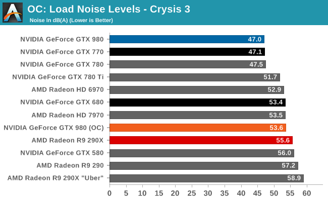
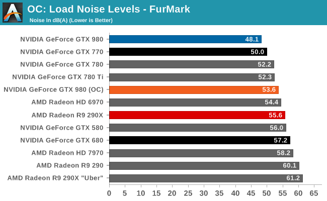
The noise penalty for overclocking is also pretty stiff. Since we're otherwise TDP limited, all of our workloads top out at 53.6dB, some 6.6dB higher than stock. In the big picture this means the overclocked GTX 980 is still in the middl of the pack, but it is noticably louder than before and louder than a few of NVIDIA's other cards. However interestingly enough it's no worse than the original stock GTX 680 at Crysis 3, and still better than said GTX 680 under FurMark. It's also still quieter than the stock Radeon R9 290X, not to mention the louder yet uber mode.


274 Comments
View All Comments
jmunjr - Friday, September 19, 2014 - link
Wish you had done a GTX 970 review as well like many other sites since way more of us care about that card than the 980 since it is cheaper.Gonemad - Friday, September 19, 2014 - link
Apparently, if I want to run anything under the sun in 1080p cranked to full at 60fps, I will need to get me one GTX 980 and a suitable system to run with it, and forget mid-ranged priced cards.That should put an huge hole in my wallet.
Oh yes, the others can run stuff at 1080p, but you have to keep tweaking drivers, turning AA on, turning AA off, what a chore. And the milennar joke, yes it RUNS Crysis, at the resolution I'd like.
Didn't, by any chance, the card actually benefit of being fabricated at 28nm, by spreading its heat over a larger area? If the whole thing, hipothetically, just shrunk to 14nm, wouldn't all that 165W of power would be dissipated over a smaller area (1/4 area?), and this thing would hit the throttle and stay there?
Or by being made smaller, it would actually dissipate even less heat and still get faster?
Yojimbo - Friday, September 19, 2014 - link
I think that it depends on the process. If Dennard scaling were to be in effect, then it should dissipate proportionally less heat. But to my understanding, Dennard scaling has broken down somewhat in recent years, and so I think heat density could be a concern. However, I don't know if it would be accurate to say that the chip benefited from the 28nm process, since I think it was originally designed with the 20nm process in mind, and the problem with putting the chip on that process had to do with the cost and yields. So, presumably, the heat dissipation issues were already worked out for that process..?AnnonymousCoward - Friday, September 26, 2014 - link
The die size doesn't really matter for heat dissipation when the external heat sink is the same size; the thermal resistance from die to heat sink would be similar.danjw - Friday, September 19, 2014 - link
I would love to see these built on Intel's 14nm process or even the 22nm. I think both Nvidia and AMD aren't comfortable letting Intel look at their technology, despite NDAs and firewalls that would be a part of any such agreement.Anyway, thanks for the great review Ryan.
Yojimbo - Friday, September 19, 2014 - link
Well, if one goes by Jen-Hsun Huang's (Nvidia's CEO) comments of a year or two ago, Nvidia would have liked Intel to manufacture their SOCs for them, but it seems Intel was unwilling. I don't see why they would be willing to have them manufacture SOCs and not GPUs being that at that time they must have already had the plan to put their desktop GPU technology into their SOCs, unless the one year delay between the parts makes a difference.r13j13r13 - Friday, September 19, 2014 - link
hasta que no salga la serie 300 de AMD con soporte nativo para directx 12Arakageeta - Friday, September 19, 2014 - link
No interpretation of the compute graphs whatsoever? Could you at least report the output of CUDA's deviceQuery tool?texasti89 - Friday, September 19, 2014 - link
I'm truly impressed with this new line of GPUs. To be able to acheive this leap on efficiency using the same transistor feature size is a great incremental achievement. Bravo TSMC & Nvidia. I feel comfortable to think that we will soon get this amazing 980 performance level on game laptops once we scale technology to the 10nm process. Keep up the great work.stateofstatic - Friday, September 19, 2014 - link
Spoiler alert: Intel is building a new fab in Hillsboro, OR specifically for this purpose...