AMD Radeon R9 285 Review: Feat. Sapphire R9 285 Dual-X OC
by Ryan Smith on September 10, 2014 2:00 PM ESTMeet The Sapphire R9 285 Dual-X OC 2GB
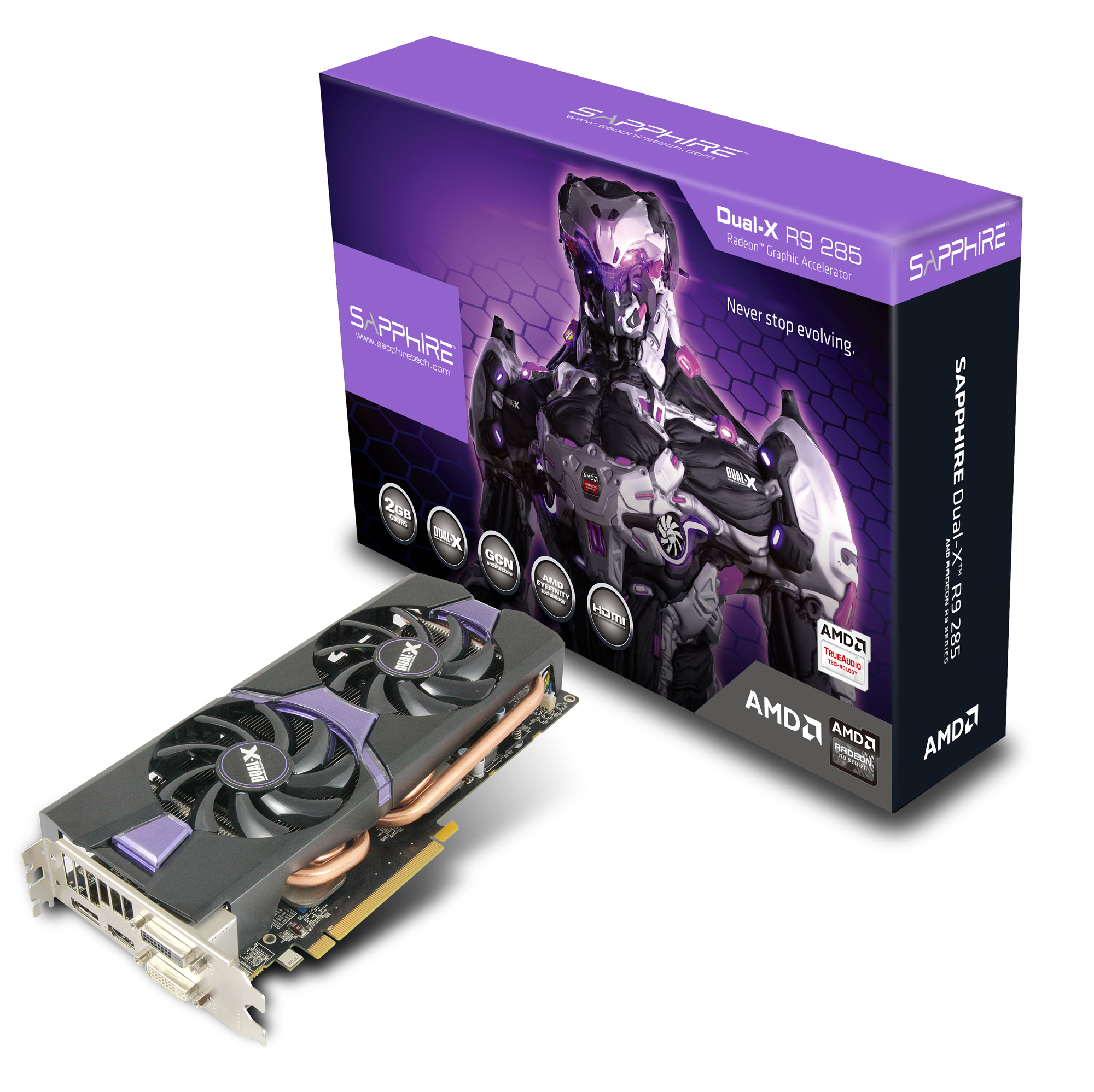
Our sample provided by AMD for today’s launch is Sapphire’s R9 285 Dual-X OC 2GB. As we mentioned before this is a non-reference launch, so rather than ship out engineering cards that won’t see retail AMD has sent us proper retail cards.
Sapphire’s R9 285 Dual-X OC is in turn a good example of what kinds of cards are appearing on store shelves. As R9 285 is a sub-200W product all of the launch cards have followed the same basic design, utilizing their manufacturer’s respective dual fan open air designs. So if you like full size open air cards then you’ll have your pick of the litter. However it also means that there aren’t any blowers on the market – nor do we expect any in the development pipeline – so for the moment the market for R9 285s is rather homogenous. In Sapphire’s case, though not available at launch, we will eventually see them break the mold with a smaller single-fan card specifically designed for use in ITX systems.
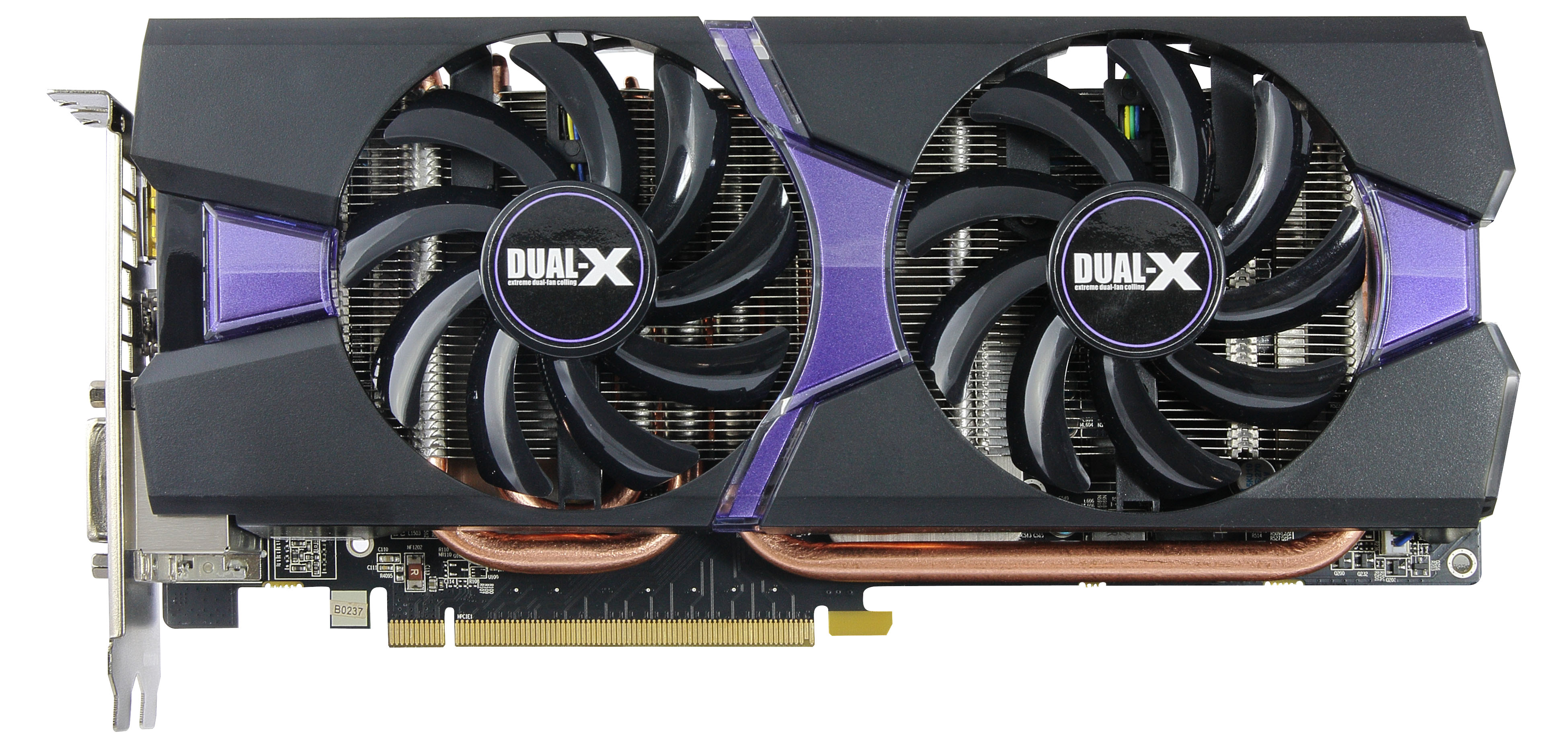
But getting to the R9 285 Dual-X OC, the Dual-X is a solid entry from Sapphire that is very typical of their current designs. As given away by the name, this card utilizes a 10” version of Sapphire’s Dual-X open-air cooler, and among Sapphire’s product lineup it can be considered the company’s baseline cooler for products up to 250W. Meanwhile as an OC model Sapphire is shipping this card with a mild factory overclock of 965MHz for the core and 5.6GHz for the memory, which represents a 47MHz (5%) core overclock and 100MHz (2%) memory overclock. Though note that Sapphire is also producing an identical version of this hardware without the factory overclock.
Continuing with our overall theme of R9 285 being a lateral product for AMD, the same is unsurprisingly true for Sapphire. For the R9 285 Dual-X Sapphire has opted to port over the design of their existing R9 280 Dual-X (which happens to be our R9 280 test card), building a suitable new PCB for Tonga but otherwise retaining the R9 280’s cooler and functionality. With R9 280 being a more power hungry part (on paper at least), this means the R9 285 Dual-X cooler is slightly overpowered in comparison, which should bode well for temperature/acoustic performance and for overclocking.
The Dual-X cooler itself is something of a tried and true design for Sapphire at this point, as years of iteration on dual fan coolers has resulted in these designs coalescing into similar and highly effective coolers. Starting from the top, the 10” version of the Dual-X cooler utilizes a pair of 85mm fans, allowing it to provide more than sufficient airflow for the primary and VRM heatsinks. Buyers with cramped cases will want to note that the use of such a large fan does result in a shroud larger than the PCB itself, with the shroud extending an additional 1cm over the PCB.
Below the fans we find Sapphire’s primary heatsink, which is composed of aluminum and runs just short of the entire length of the cooler. Sapphire attaches the primary heatsink to the GPU through the use of 4 copper heatpipes which run between the GPU and various points on the heatsink. The heatpipes in turn do not make direct contact with the GPU, but instead attach to a copper baseplate which in turn is what makes contact with the GPU and channels heat into the heatpipes.
Surrounding the copper baseplate is a secondary aluminum baseplate which provides both structure for the overall heatsink and additional cooling. Through the use of thermal pads, the aluminum baseplate covers the card’s RAM chips, providing direct cooling for the RAM. Meanwhile the card’s VRMs are not part of the primary heatsink assembly, and are instead cooled via a smaller secondary “strip” heatsink that sits over the MOSFETs towards the rear of the card. Airflow making it through the primary heatsink is in turn responsible for cooling this secondary heatsink.
Removing the heatsink and accessing the PCB, Sapphire’s PCB is typical for a 200W card. Sapphire places the bulk of the VRM circuitry towards the rear of the card, between the GPU/RAM and the PCIe power sockets. Meanwhile Sapphire’s RAM of choice is 6GHz Elpedia, which means this card ships at a lower memory frequency than what the RAM is capable of. For overclockers this means there’s some guaranteed headroom on the RAM, while the lower shipping frequency may indicate that AMD has tuned Tonga’s memory controllers for sub-6GHz operation, similar to what happened with Hawaii.
Throughout all of this the R9 285 Dual-X OC is generally a solid card, but the heatsink/PCB interaction does expose the card’s one real weakness/design flaw, which is a lack of rigidity. As is almost always the case with these large heatsink cards, the heatsink is massive enough that for all practical purposes the PCB is attached to the heatsink rather than vice versa. However Sapphire only attaches the heatsink to the PCB at the 4 screws around the GPU, which for a 10.25” card means the far end of the card is far removed from these attachment points and is left free to flex. Sapphire does include a plastic leg at one corner of the shroud to keep the PCB from flexing too much, but this leg isn’t secured to the PCB and indeed isn’t even long enough to touch the PCB without flexing. Ideally we would like to see all 9”+ cards reinforced against flexing for this reason, either by securing the shroud to the PCB at the rear of the card or by employing a stiffener along the top edge of the PCB.
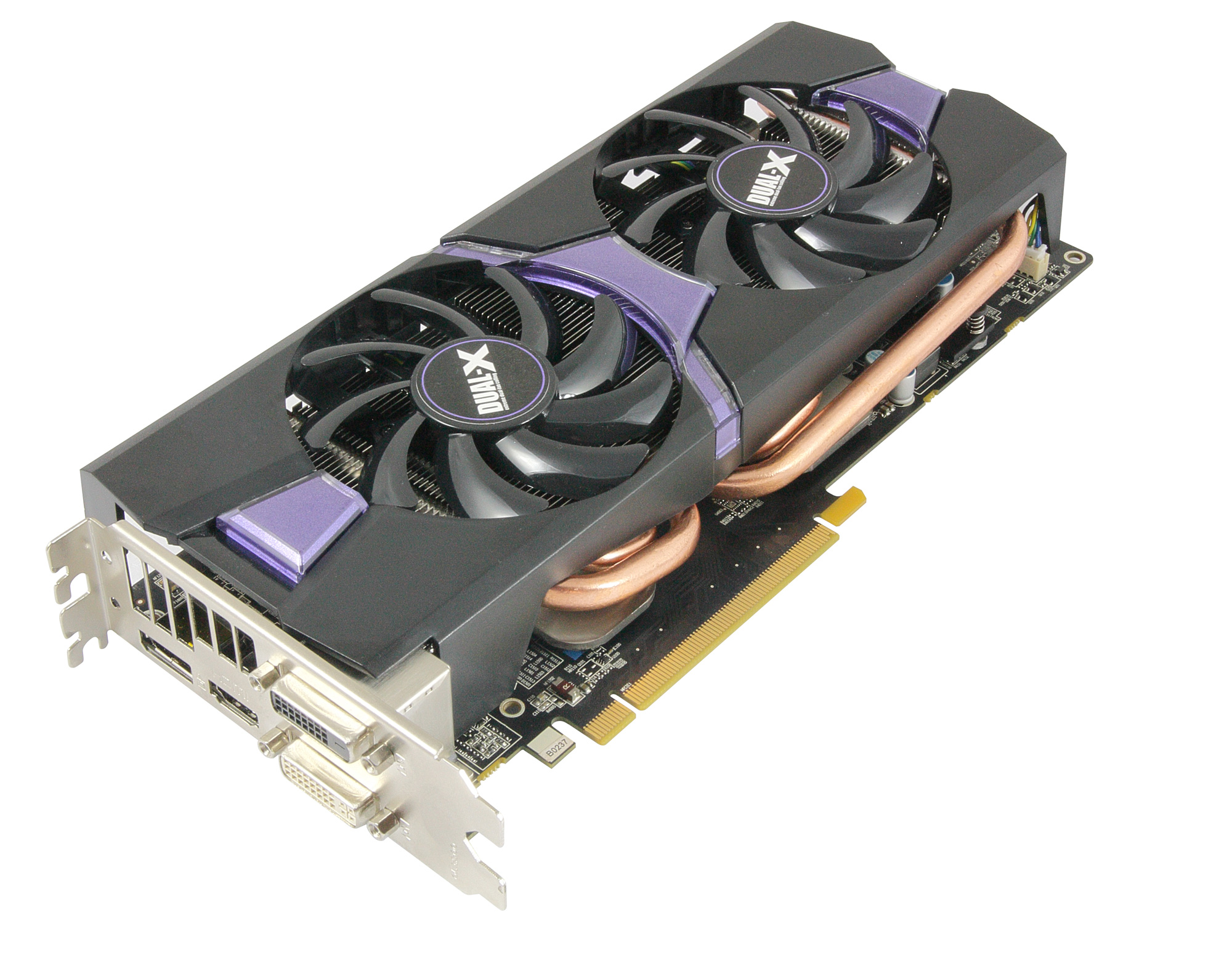
Moving on, Sapphire doesn’t list an official TDP for the R9 285 Dual-X OC, however given the factory overclock it’s fair to say that in practice it’s going to be a bit higher than AMD’s official 190W TDP of a stock R9 285. Providing power for the card is a pair of 6pin PCIe power connectors at the top-rear of the card, which along with the PCIe slot connector means the card has the means to deliver up to 225W of power (VRMs willing). Interestingly Sapphire’s PCB has an additional pair of solder points for replacing one of the 6pin connectors with an 8pin connector, which may indicate a future Sapphire card or Sapphire hedging their bets for the inevitable higher tier Tonga card with all 32 CUs enabled.
Meanwhile though you won’t find a Crossfire connector at the top of the card – having been made obsolete by GCN 1.1+’s XDMA engines – what you will find on the Sapphire card is a BIOS switch. Sapphire ships the R9 285 Dual-X as a dual BIOS UEFI card, with one BIOS for legacy systems and a second BIOS for UEFI systems. The card’s default shipping state will be for the legacy BIOS, while depressing the BIOS button will switch to UEFI. Outside of reference cards we don’t see too many dual BIOS cards, and given the limited selection of such cards we are rather fond of the fact that Sapphire uses a button here as opposed to a more difficult to access switch.
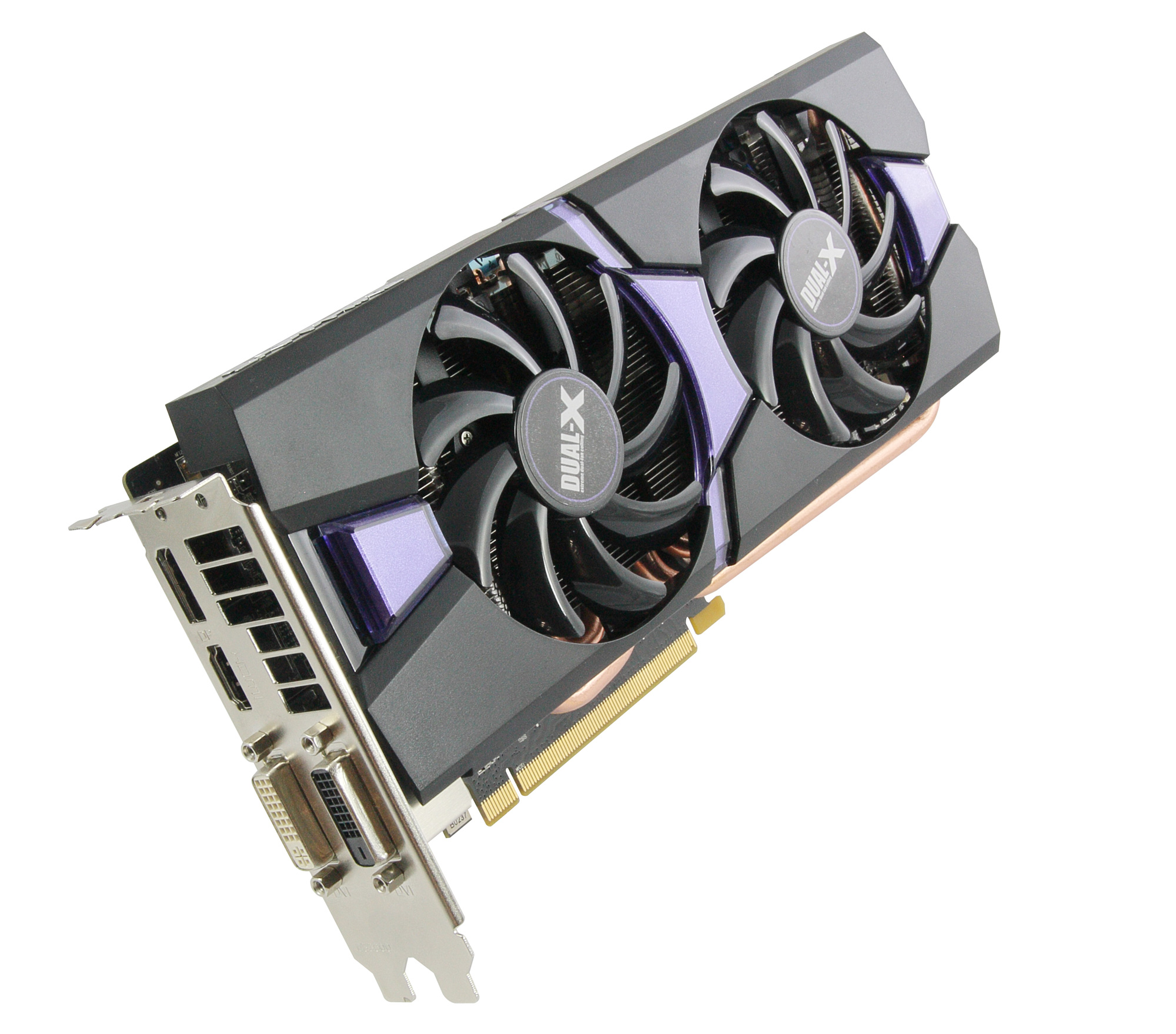
Finally, towards the front of the card we see the standard AMD 200 series I/O configuration of 1x DL-DVI-I, 1x DL-DVI-D, 1x HDMI, and 1x DisplayPort. Tonga has up to 6 display controllers, and while not easy it should be possible to use all 6 of them through a careful use of MST off of the DisplayPort and identical monitors hanging off of the HDMI and DVI ports.
Wrapping things up, the retail price on the R9 285 Dual-X OC is currently running at $259. This puts Sapphire’s card at $10 over the R9 285 MSRP of $249, though given the fact that this is a factory overclocked card this is par for the course. We haven’t seen the non-OC version for sale yet, but one way or another you’re essentially looking at paying a 4% price premium for roughly as much of a performance advantage over a stock R9 285.


86 Comments
View All Comments
chizow - Thursday, September 11, 2014 - link
If Tonga is a referendum on Mantle, it basically proves Mantle is a failure and will never succeed. This pretty much shows most of what AMD said about Mantle is BS, that it takes LESS effort (LMAO) on the part of the devs to implement than DX.If Mantle requires both an application update (game patch) from devs AFTER the game has already run past its prime shelf-date AND also requires AMD to release optimized drivers every time a new GPU is released, then there is simply no way Mantle will ever succeed in a meaningful manner with that level of effort. Simply put, no one is going to put in that kind of work if it means re-tweaking every time a new ASIC or SKU is released. Look at BF4, its already in the rear-view mirror from DICE's standpoint, and no one even cares anymore as they are already looking toward the next Battlefield#
TiGr1982 - Thursday, September 11, 2014 - link
Please stop calling GPUs ASICs - this looks ridiculous.Please go to Wikipedia and read what "ASIC" is.
chizow - Thursday, September 11, 2014 - link
Is this a joke or are you just new to the chipmaking industry? Maybe you should try re-reading the Wikipedia entry to understand GPUs are ASICs despite their more recent GPGPU functionality. GPU makers like AMD and Nvidia have been calling their chips ASICs for decades and will continue to do so, your pedantic objections notwithstanding.But no need to take my word for it, just look at their own internal memos and job listings:
https://www.google.com/#q=intel+asic
https://www.google.com/#q=amd+asic
https://www.google.com/#q=nvidia+asic
TiGr1982 - Thursday, September 11, 2014 - link
OK, I accept your arguments, but I still don't like this kind of terminology. To me, one may call things like fixed-function video decoder "ASIC" (for example UVD blocks inside Radeon GPUs), but not GPU as a whole, because people do GPGPU for a number of years on GPUs, and "General Purpose" in GPGPU contradicts with "Aplication Specific" in ASIC, isn't it?So, overall it's a terminology/naming issue; everyone uses the naming whatever he wants to use.
chizow - Thursday, September 11, 2014 - link
I think you are over-analyzing things a bit. When you look at the entire circuit board for a particular device, you will see each main component or chip is considered an ASIC, because each one has a specific application.For example, even the CPU is an ASIC even though it handles all general processing, but its specific application for a PC mainboard is to serve as the central processing unit. Similarly, a southbridge chip handles I/O and communications with peripheral devices, Northbridge handles traffic to/from CPU and RAM and so on and so forth.
TiGr1982 - Thursday, September 11, 2014 - link
OK, then according to this (broad) understanding, every chip in silicon industry may be called ASIC :)Let it be.
chizow - Friday, September 12, 2014 - link
Yes, that is why everyone in the silicon industry calls their chips that have specific applications ASICs. ;)Something like a capacitor, or resistor etc. would not be as they are of common commodity.
Sabresiberian - Thursday, September 11, 2014 - link
I reject the notion that we should be satisfied with a slower rate of GPU performance increase. We have more use than ever before for a big jump in power. 2560x1440@144Hz. 4K@60Hz.Of course it's all good for me to say that without being a micro-architecture design engineer myself, but I think it's time for a total re-think. Or if the companies are holding anything back - bring it out now, please! :)
Stochastic - Thursday, September 11, 2014 - link
Process node shrinks are getting more and more difficult, equipment costs are rising, and the benefits of moving to a smaller node are also diminishing. So sadly I think we'll have to adjust to a more sedate pace in the industry.TiGr1982 - Thursday, September 11, 2014 - link
I'm a longstanding AMD Radeon user for more than 10 years, but after reading this R9 285 review I can't help but think that, based on results of smaller GM107 in 750 Ti, GM204 in GTX 970/980 may offer much better performance/Watt/die area (at least for gaming tasks) in comparison to the whole AMD GPU lineup. Soon we'll see whether or not this will be the case.