AMD Radeon R9 285 Review: Feat. Sapphire R9 285 Dual-X OC
by Ryan Smith on September 10, 2014 2:00 PM ESTSynthetics
As always we’ll also take a quick look at synthetic performance. As we briefly discussed in our look at the GCN 1.2 architecture these tests mainly serve as a canary for finding important architectural changes, and one of these tests in particular has been significantly impacted by AMD’s newest round of architectural improvements.
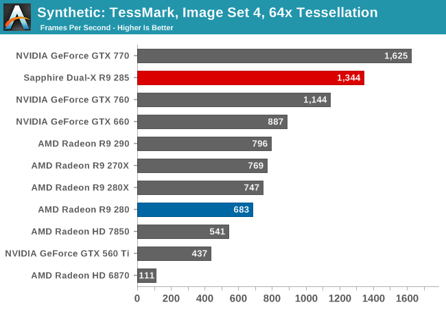
At the x64 tessellation factor we see the R9 285 spit out 134fps, or equivalent to roughly 1.47B polygons/second. This is as compared to 79fps (869M Polys/sec) for the R9 290, and 68fps (748M Polys/sec) for the R9 280. One of the things we noted when initially reviewing the R9 290 series was that AMD’s tessellation performance didn’t pick up much in our standard tessellation benchmark (Tessmark at x64) despite the doubling of geometry processors, and it looks like AMD has finally resolved that with GCN 1.2’s efficiency improvements. As this is a test with a ton of small triangles, it looks like we’ve hit a great case for the vertex reuse optimizations.
Moving on, we have our 3DMark Vantage texture and pixel fillrate tests, which present our cards with massive amounts of texturing and color blending work. These aren’t results we suggest comparing across different vendors, but they’re good for tracking improvements and changes within a single product family.
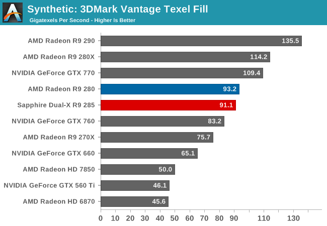
With AMD maintaining their same texture units and same tex:FP32 ratio for Tonga, the end result is that R9 285’s texturing performance is virtually identical to R9 280’s. Ignoring any possibility of caching or bandwidth bottlenecking for the moment, R9 285 can push texels just as well as R9 280 could.
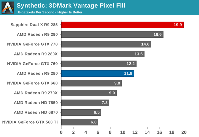
Unlike our texel test, AMD’s delta color compression technology introduced on GCN 1.2 has an incredible impact on R9 285’s pixel throughput. This pixel test is normally memory bandwidth bound, providing something that approaches a best case scenario for AMD’s compression technology. As a result despite possessing nearly 30% less memory bandwidth than the R9 280, the R9 285 tops our charts at 19.9 GPix/sec, blowing past the R9 280 by 68%. Even the R9 290 with its 512-bit memory bus and doubled ROP count still falls short here by over 3GPix/sec, or 16%.
This benchmark in a nutshell is why AMD can deliver the average performance of the Tahiti based R9 280 without Tahiti’s memory bandwidth. By improving their color compression to this point AMD can significantly reduce their memory bandwidth requirements on GCN 1.2, allowing them to do more with less. In real games the result won’t be anywhere near this remarkable since this is a pure pixel fillrate test, but it goes to show that AMD has been able to neutralize their memory bandwidth deficit in graphics workloads.


86 Comments
View All Comments
chizow - Thursday, September 11, 2014 - link
If Tonga is a referendum on Mantle, it basically proves Mantle is a failure and will never succeed. This pretty much shows most of what AMD said about Mantle is BS, that it takes LESS effort (LMAO) on the part of the devs to implement than DX.If Mantle requires both an application update (game patch) from devs AFTER the game has already run past its prime shelf-date AND also requires AMD to release optimized drivers every time a new GPU is released, then there is simply no way Mantle will ever succeed in a meaningful manner with that level of effort. Simply put, no one is going to put in that kind of work if it means re-tweaking every time a new ASIC or SKU is released. Look at BF4, its already in the rear-view mirror from DICE's standpoint, and no one even cares anymore as they are already looking toward the next Battlefield#
TiGr1982 - Thursday, September 11, 2014 - link
Please stop calling GPUs ASICs - this looks ridiculous.Please go to Wikipedia and read what "ASIC" is.
chizow - Thursday, September 11, 2014 - link
Is this a joke or are you just new to the chipmaking industry? Maybe you should try re-reading the Wikipedia entry to understand GPUs are ASICs despite their more recent GPGPU functionality. GPU makers like AMD and Nvidia have been calling their chips ASICs for decades and will continue to do so, your pedantic objections notwithstanding.But no need to take my word for it, just look at their own internal memos and job listings:
https://www.google.com/#q=intel+asic
https://www.google.com/#q=amd+asic
https://www.google.com/#q=nvidia+asic
TiGr1982 - Thursday, September 11, 2014 - link
OK, I accept your arguments, but I still don't like this kind of terminology. To me, one may call things like fixed-function video decoder "ASIC" (for example UVD blocks inside Radeon GPUs), but not GPU as a whole, because people do GPGPU for a number of years on GPUs, and "General Purpose" in GPGPU contradicts with "Aplication Specific" in ASIC, isn't it?So, overall it's a terminology/naming issue; everyone uses the naming whatever he wants to use.
chizow - Thursday, September 11, 2014 - link
I think you are over-analyzing things a bit. When you look at the entire circuit board for a particular device, you will see each main component or chip is considered an ASIC, because each one has a specific application.For example, even the CPU is an ASIC even though it handles all general processing, but its specific application for a PC mainboard is to serve as the central processing unit. Similarly, a southbridge chip handles I/O and communications with peripheral devices, Northbridge handles traffic to/from CPU and RAM and so on and so forth.
TiGr1982 - Thursday, September 11, 2014 - link
OK, then according to this (broad) understanding, every chip in silicon industry may be called ASIC :)Let it be.
chizow - Friday, September 12, 2014 - link
Yes, that is why everyone in the silicon industry calls their chips that have specific applications ASICs. ;)Something like a capacitor, or resistor etc. would not be as they are of common commodity.
Sabresiberian - Thursday, September 11, 2014 - link
I reject the notion that we should be satisfied with a slower rate of GPU performance increase. We have more use than ever before for a big jump in power. 2560x1440@144Hz. 4K@60Hz.Of course it's all good for me to say that without being a micro-architecture design engineer myself, but I think it's time for a total re-think. Or if the companies are holding anything back - bring it out now, please! :)
Stochastic - Thursday, September 11, 2014 - link
Process node shrinks are getting more and more difficult, equipment costs are rising, and the benefits of moving to a smaller node are also diminishing. So sadly I think we'll have to adjust to a more sedate pace in the industry.TiGr1982 - Thursday, September 11, 2014 - link
I'm a longstanding AMD Radeon user for more than 10 years, but after reading this R9 285 review I can't help but think that, based on results of smaller GM107 in 750 Ti, GM204 in GTX 970/980 may offer much better performance/Watt/die area (at least for gaming tasks) in comparison to the whole AMD GPU lineup. Soon we'll see whether or not this will be the case.