MIPS Strikes Back: 64-bit Warrior I6400 Arrives
by Stephen Barrett on September 2, 2014 10:00 AM ESTThe MIPS I6400 CPU
Like the Cortex-A53, the I6400 is an in-order, dual-issue design. Each processor supports IEEE 754-2008 floating point operations, 128-bit SIMD instructions, and hardware virtualization. ARM has previously stated that Cortex-A9 is roughly 2.5 mm2 of area with a 40 nm process, and Cortex-A53 is 40% smaller at the same process, placing it at roughly 1.5 mm2 of area. At 28nm, we can estimate a Cortex-A53 is about 1mm2. Comparatively, MIPS states the I6400 is 1mm2 on the TSMC 28nm HPM process in "worst-case scenarios". Therefore the designs are quite comparable.
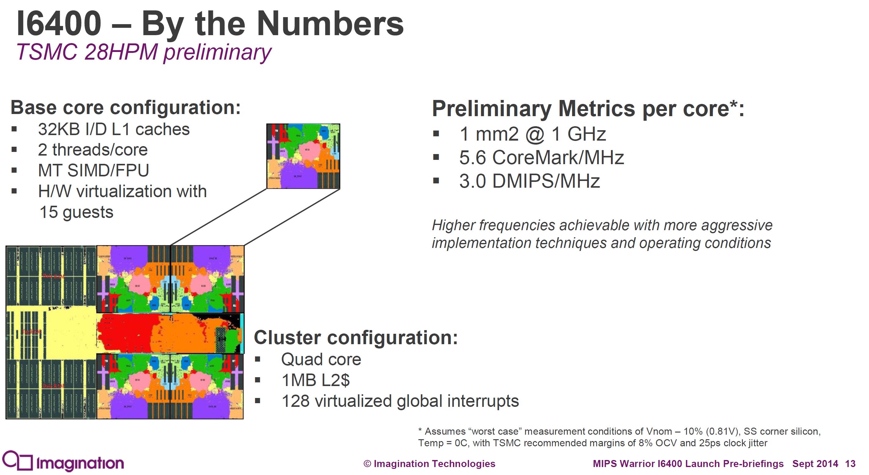
Differences between the Cortex-A53 and I6400 start with a 9 stage pipeline in the I6400 vs 8 stages with the A53, theoretically allowing the I6400 to clock higher. However the I6400 is 9 stages for all operations, whereas the A53 is 8 stages for integer but 10 for NEON/Floating Point operations.
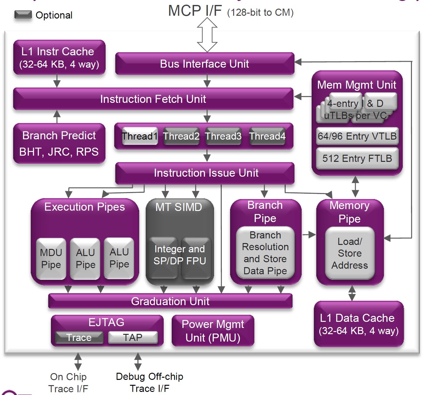
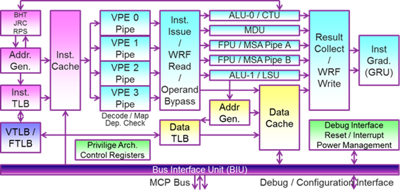
If you look closely at the block diagram you can see one of the I6400’s interesting tricks: Simultaneous Multi-Threading (SMT). Avid readers of AnandTech should recognize this technology immediately. It has been utilized by Intel since the venerable Pentium 4, over a decade ago in 2002, under the trademarked name Hyper-Threading. While the Core Duo and Core 2 lines dropped support for Hyper-Threading, the Nehalem (Core i7) and later processors have continued its use. IBM's POWER cores also support SMT (up to 4-way SMT with POWER7 and 8-way SMT with POWER8).
Strangely, we have not seen anyone else (e.g. ARM or AMD) implement this same technology until now. AMD has a partial implementation in its Bulldozer architecture, with each "module" in their current CPUs/APUs providing two full integer cores with some shared elements. AMD contends that their partial SMT implementation is actually better for some workloads, but that's a different discussion. Regardless, SMT support it is new to the small-core space.
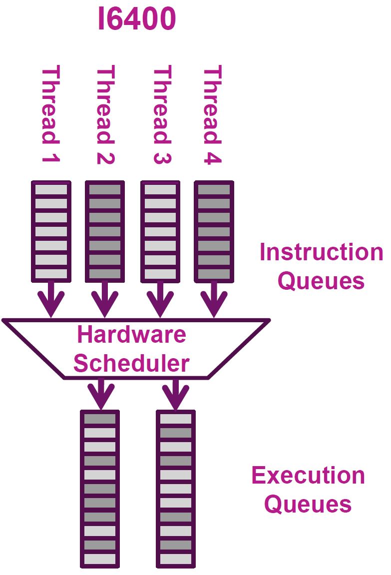
An SoC designer licensing an I6400 core can decide how many threads of SMT they want to implement into the core, from 1 to 4. The physical core then advertises itself to the operating system as 1 to 4 logical cores, thus allowing the OS to send up to four threads of instructions to execute at any given time. The hardware’s execution scheduler can then, per cycle, dynamically switch between threads depending on which hardware resources are available. For example, if the integer ALUs are tied up with threads 1-3 but thread 4 only needs floating point resources, the scheduler can schedule thread 4 to the FP units instead of waiting around.
Imagination claims their MIPS core featuring SMT only increases 10% in size but increases an incredible 30% to 50% in performance. A 3x to 5x size to performance ratio for any given feature is quite hard to come by. If Imagination’s claims are correct, it’s a wonder this feature is optional. Certain applications greatly suffer from SMT, namely real-time applications that depend on determinism, but like Intel Hyper-Threading, I would hope there is a simple software setting to disable this feature when it is not desired. Imagination specifically calls out networking applications (which are very throughput focused) as greatly benefiting from SMT, which is the optional MIPS MT extension.
Even though the core is in-order, the I6400 performs superscalar execution for a given thread. Since it is dual dispatch, two instructions from a single thread can be executed in parallel. I would imagine the superscalar execution is limited to the next two instructions within a thread (as there is no reorder buffer); otherwise the entire core wouldn’t be listed as in-order.
| Mid-Class CPU Core Comparison | ||||||
| MIPS I6400 | ARM Cortex-A53 | |||||
| CPU Codename | Warrior | Apollo | ||||
| ISA | MIPS3264 Release 6 | ARMv8-A (32/64-bit) | ||||
| Cores in an SMP Cluster | 1-6 | 1-4 | ||||
| Thread Width | 1-4 | 1 | ||||
| Issue Width | 2 micro-ops | 2 micro-ops | ||||
| Reorder Buffer Size | None: In-Order | None: In-Order | ||||
| Pipeline Depth (stages) | 9 | 8 (Int) 10 (FP) | ||||
| Integer ALUs | 2 | 2 | ||||
| Load/Store Units | 1 (2 with bonding) | 1 | ||||
| Load Latency | 3 cycles | 3 cycles | ||||
| Branch Units | 1 | 1 | ||||
| FP/NEON ALUs | 2 | 2 | ||||
| Coherency | Directory | Snoop + Filter | ||||
| L1 Cache | 32 or 64KB I$ + 32 or 64KB D$ | 8 to 64KB I$ + 8 to 64KB D$ | ||||
| L2 Cache | 0.5 to 8MB | 0.5 to 2MB | ||||
Another trick the I6400 employs is called instruction bonding or load/store bonding, which probably ties in with the previously mentioned hardware scheduler. If two load or store instructions arrive at the scheduler with adjacent addresses, the I6400 can "bond" them together into a single instruction executed by the load/store unit. Two 32-bit integer accesses will be bonded into a single 64-bit integer access, two 64-bit integer accesses bond into a single 128-bit integer access, and two 64-bit floating point accesses bond into a single 128-bit FP access.
Applications often perform memcopies that move relatively large amounts of memory from point A to point B, resulting in a long list of load/store instructions. This hardware scheduler feature can halve the time required to fulfill a memcopy request and is completely transparent to software. MIPS states this feature is a natural expansion of their load/store unit, as their bus widths are already 128-bits to support their SIMD unit. Doubling the efficiency of the I6400's single load/store unit (in certain cases) helps save area and power compared to duplicating the unit entirely.
Directory Based Coherency
One of the largest problems a multicore processor needs to solve is coherency. Multiple PhDs have been earned on this topic alone. The core of the problem (pun intended) is that multiple execution resources (CPU or GPU cores) exist each with their own L1 data cache. If Core1 writes to address 0xABC0FF, its L1 data cache is immediately updated. However, what if there is another core present that also has the data at address 0xABC0FF cached? Its cached data is now invalid and, if used, results in computational inconsistency and a potentially critical application errors.
There are multiple techniques to deal with this problem. The most common is called snooping. Each core in a multicore system monitors the L1 cache lines of every other core. If a write is observed to an address that is locally cached, that cache line is immediately invalidated. When an invalidated cache line is accessed, the invalid data is not returned but rather a longer trip out to the coherent L2 cache is made. Since all the L1 caches update whenever any L1 cache is written to, this is the most performant coherency implementation. However, it is quite complex. If eight cores are designed with coherent L1 caches, each core must connect to seven other cores, causing an explosion of complexity.
One way modern designs deal with increasing snoop complexity is by using a "snoop bus". Instead of connecting all cores L1 caches to each other, all cores are connected all to a shared bus. When a core writes to an L1 cache location, it broadcasts the address written to all other cores on the snoop bus. Other cores then invalidate that address if it is present in their L1 cache. This helps with wiring inside the chip, but snoop traffic is still increasing with added cores. ARM's A53 goes a step further and has a Snoop Control Unit (SCU) that sits on the bus and filters out snoop traffic based upon which caches have which addresses.
The I6400 uses the other common technique, directory based coherency. The L2 cache in the I6400 maintains a listing of all the data being duplicated in attached CPU cores. When an address is changed, the directory is always notified. The directory can then update the attached CPU cores that have duplicated that data. In the worst-case scenario this is both higher latency (informing the directory of a write takes time) and can result in increased bus traffic because every core could have cached a particular address. However, it’s not likely that every single core would have cached the same data that gets overwritten. Either way, it is significantly simpler to implement as it is a single point to point connection between L1 and L2 per core rather than a web of connections between L1s. This is likely a contributing factor in why the I6400 can be used in SMP clusters of 6, whereas the A53 is limited to SMP clusters of 4.

Finally, the I6400 includes fine grained power consumption optimizations branded as “PowerGearing” by MIPS. The processor can disable clocks (clock gating) to individual CPU cores, caches, and subsystems (such as SIMD blocks). Each CPU core can individually sleep and be controlled by OS Dynamic Voltage and Frequency Scaling (DVFS), which is essential to Android/Linux processor power management.


84 Comments
View All Comments
alexvoica - Tuesday, September 2, 2014 - link
You've (almost too) carefully forgot to mention the trap-and-emulate feature described in the spec.DMStern - Tuesday, September 2, 2014 - link
The documentation also says that only a subset can be trapped, and that some encodings have been re-used. I haven't studied the instruction encoding tables closely enough to know how many, and how serious the conflicts are. Presumably, as more instructions are added in later revisions, the less useful trapping will be.Daniel Egger - Tuesday, September 2, 2014 - link
Finally! I've been waiting a long time for new decent MIPS processors to show up as I've never quite warmed up with the ARM ISA.However the introduction is missing a couple of important facts (probably even more):
1) RISC is usually a load-and-store architecture, meaning there're registers in abundance and the only way to work with data is to load it into registers and store it back if the result is needed later
2) ... and that's also the reason why the instruction set is much simpler because there're less instruction variants because source and targets are known to be registers and in few cases immediates but almost never those funky combinations of different memory access types one can find in CISC
3) This also means that instruction size is constant on RISC vastly simplifying instruction fetching and decoding
4) Whether the code size increases or decreases compared to CISC very much depends on how the application and compiler can utilize the available registers because most of the bloat in RISC is actually caused by loads and stores, however thanks to register starvation on x86 there might be lots of cases where the addressing causes lots of bloat
I would say if there's a comparison between RISC and CISC it should be more detailed on the important differences. Otherwise, why bother at all?
darkich - Tuesday, September 2, 2014 - link
Great, but unfortunately for Imagination, ARM have already started licensing the successors to Cortex A53 and A57.They are codenamed Artemis and Maya
darkich - Tuesday, September 2, 2014 - link
..a bit of clarification, the Artemis refers to the big core while Maya is the small onetuxRoller - Tuesday, September 2, 2014 - link
Great article Stephen.Could you, at some point, go into a bit more depth on the relationships between out of order, superscalar and simultaneous multithreading? Your description of the dispatcher, and classification of this core as in-order, makes me wonder if I understand it at all. In particular, I didn't realise that superscalar is just a special case of out of order, as your text seems to imply (though you do say that it is not out of order, so it is puzzling).
heartinpiece - Tuesday, September 2, 2014 - link
Some inaccurate information:Snoop coherence protocol doesn't connect cores to other cores, or one core doesn't monitor cache lines of another core.
Instead coherence messages are broadcast to all cores of the system, and each core checks whether it has the cache that was broadcasted, and takes appropriate actions.
If 8 cores use snooping, they don't 'connect' to the other 7, but rather the amount of broadcasted coherence messages increases. (Which may clog the interconnect)
In the directory protocol, when a data is updated, the directory notifies the other cores which hold the data to the same address to invalidate the corresponding cache lines (instead of filling the other cores with the updated value).
The reason for such action is because sending the actual value would be too large, and also, even if it is updated in the other cores, if the other cores don't access the newly updated cacheline, then we have sent the updated value for no reason.
Rather, the invalidated approach takes a lazier approach and only fetches the updated value upon read/write to the cacheline.
Exophase - Wednesday, September 3, 2014 - link
More on snooping in Cortex-A53:"Each core has tag and dirty RAMs that contain the state of the cache line. Rather than access these for each snoop request the SCU contains a set of duplicate tags that permit each coherent data request to be checked against the contents of the other caches in the cluster. The duplicate tags filter coherent requests from the system so that the cores and system can function efficiently even with a high volume of snoops from the system."
Stephen Barrett - Wednesday, September 3, 2014 - link
Interesting! Thank you for this detail. I tried to find info about the SCU but I couldn't and my ARM contacts had not gotten back to me yet. I've added a paragraph about thistuxRoller - Wednesday, September 3, 2014 - link
You might also want to update this sentence as the reasoning no longer seems to apply:"This is likely a contributing factor in why the I6400 can be used in SMP clusters of 6, whereas the A53 is limited to SMP clusters of 4."