The Intel Haswell-E CPU Review: Core i7-5960X, i7-5930K and i7-5820K Tested
by Ian Cutress on August 29, 2014 12:00 PM ESTEvolution in Performance
The underlying architecture in Haswell-E is not anything new. Haswell desktop processors were first released in July 2013 to replace Ivy Bridge, and at the time we stated an expected 3-17% increase, especially in floating point heavy benchmarks. Users moving from Sandy Bridge should expect a ~20% increase all around, with Nehalem users in the 40% range. Due to the extreme systems only needing more cores, we could assume that the suggested recommendations for Haswell-E over IVB-E and the others were similar but we tested afresh for this review in order to test those assumptions.
For our test, we took our previous CPU review samples from as far back as Nehalem. This means the i7-990X, i7-3960X, i7-4960X and the Haswell-E i7-5960X.
Each of the processors were set to 3.2 GHz on all the cores, and set to four cores without HyperThreading enabled.
Memory was set to the CPU supported frequency at JEDEC settings, meaning that if there should Intel have significantly adjusted the performance between the memory controllers of these platforms, this would show as well. For detailed explanations of these tests, refer to our main results section in this review.

Average results show an average 17% jump from Nehalem to SNB-E, 7% for SNB-E to IVB-E, and a final 6% from IVB-E to Haswell-E. This makes for a 31% (rounded) overall stretch in three generations.
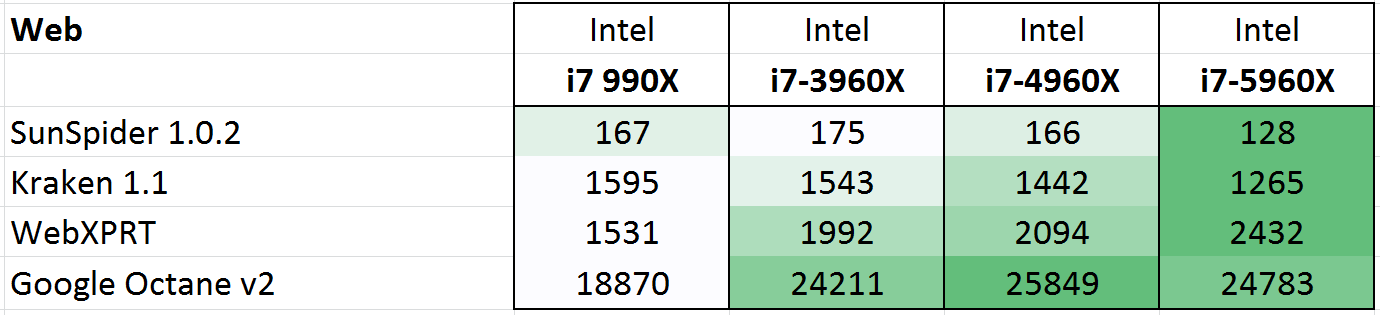
Web benchmarks have to struggle with the domain and HTML 5 offers some way to help use as many cores in the system as possible. The biggest jump was in SunSpider, although overall there is a 34% jump from Nehalem to Haswell-E here. This is split by 14% Nehalem to SNB-E, 6% SNB-E to IVB-E and 12% from IVB-E to Haswell-E.
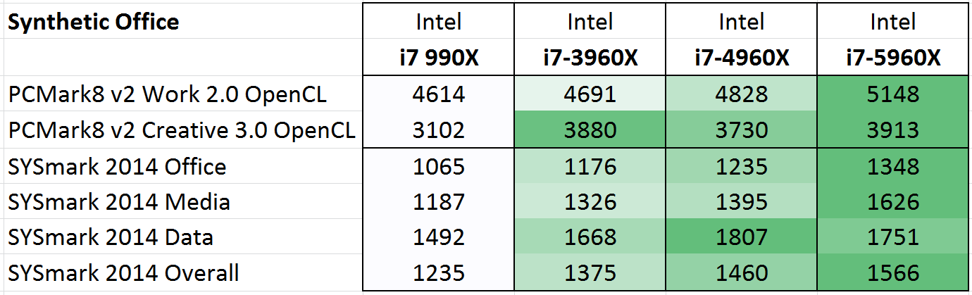
Purchasing managers often look to the PCMark and SYSmark data to clarify decisions and the important number here is that Haswell-E took a 7% average jump in scores over Ivy Bridge-E. This translates to a 24% jump since Nehalem.
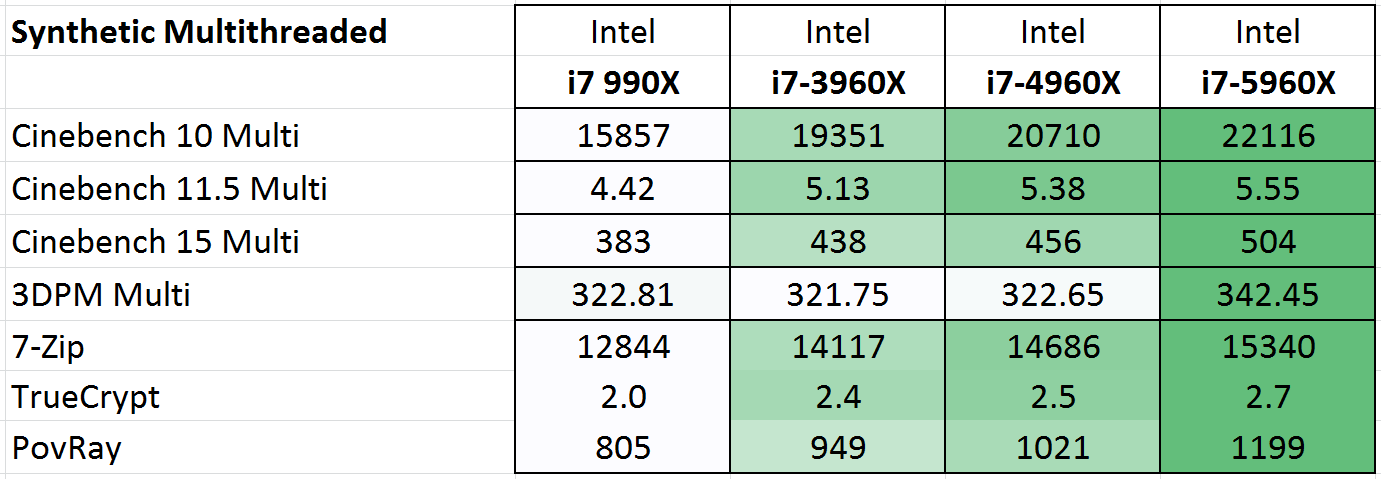
Some of the more common synthetic benchmarks in multithreaded mode showed an average 8% jump from Ivy Bridge-E, with a 29% jump overall. Nehalem to Sandy Bridge-E was a bigger single jump, giving 14% average.
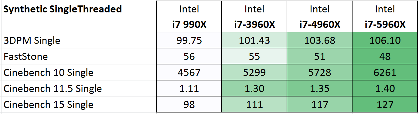
In the single threaded tests, a smaller overall 23% improvement was seen from the i7-990X, with 6% in this final generation.
The take home message, if there was one, from these results is that:
Haswell-E has an 8% improvement in performance over Ivy Bridge-E clock for clock for pure CPU based workloads.
This also means an overall 13% jump from Sandy Bridge-E to Haswell-E.
From Nehalem, we have a total 28% raise in clock-for-clock performance.
Looking at gaming workloads, the difference shrinks. Unfortunately our Nehalem system decided to stop working while taking this data, but we can still see some generational improvements. First up, a GTX 770 at 1080p Max settings:
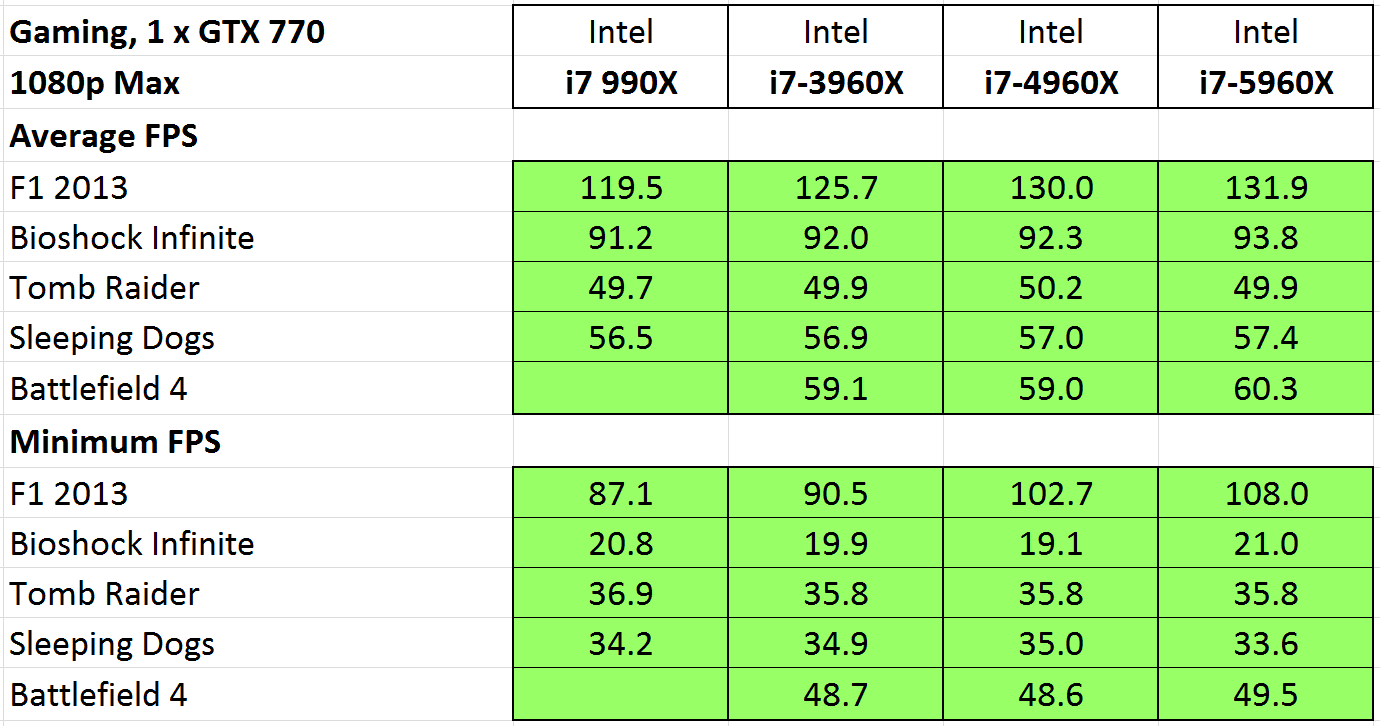
The only title that gets much improvement is F1 2013 which uses the EGO engine and is most amenable to better hardware under the hood. The rise in minimum frame rates is quite impressive.
For SLI performance:
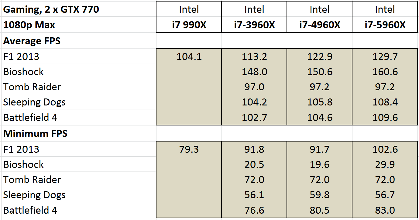
All of our titles except Tomb Raider get at least a small improvement in our clock-for-clock testing with this time Bioshock also getting in on the action in both average and minimum frame rates.
If we were to go on clock-for-clock testing alone, these numbers do not particularly show a benefit from upgrading from a Sandy Bridge system, except in F1 2013. However our numbers later in the review for stock and overclocked speeds might change that.
Memory Latency and CPU Architecture
Haswell is a tock, meaning the second crack at 22nm. Anand went for a deep dive into the details previously, but in brief Haswell bought better branch prediction, two new execution ports and increased buffers to feed an increased parallel set of execution resources. Haswell adds support for AVX2 which includes an FMA operation to increase floating point performance. As a result, Intel doubled the L1 cache bandwidth. While TSX was part of the instruction set as well, this has since been disabled due to a fundamental silicon flaw and will not be fixed in this generation.
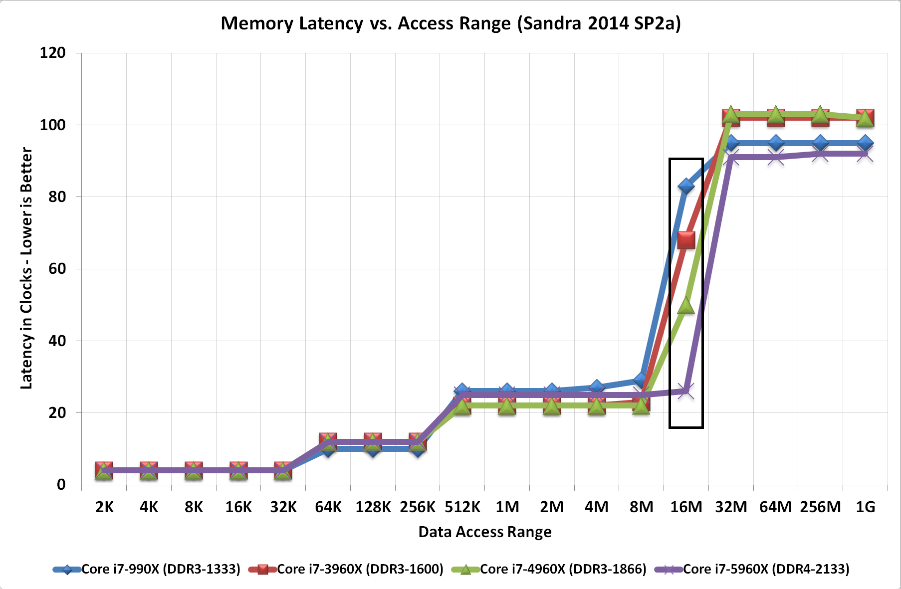
The increase in L3 cache sizes for the highest CPU comes from an increased core count, extending the lower latency portion of the L3 to larger data accesses. The move to DDR4 2133 C15 would seem to have latency benefits over previous DDR3-1866 and DDR3-1600 implementations as well.


203 Comments
View All Comments
Ian Cutress - Monday, September 1, 2014 - link
When I tested the 5930K/5820K, the motherboard BIOSes were still very early alpha builds and did not allow overclocking. If I can get these CPUs in again to test (they had to be sent back), I will do some overclocking results for sure.jwcalla - Friday, August 29, 2014 - link
Might as well wait for them to fix TSX at this point.iwod - Friday, August 29, 2014 - link
How likely will this be in Mac Pro?DigitalFreak - Friday, August 29, 2014 - link
Doubtful. Apple is using Xeons in the Mac Pro.hansmuff - Friday, August 29, 2014 - link
I'll be waiting for two more generations. Maybe something worthwhile comes along to replace my 2600k at 4.4GHz. I'm glad the review shows so clearly where this new chip excels and who should save their money.Yuriman - Friday, August 29, 2014 - link
Typo:"Modules should be available from DDR3-2133 to DDR3-3200 at launch, with the higher end of the spectrum being announced by both G.Skill and Corsair. See our DDR4 article later this week for more extensive testing."
TelstarTOS - Friday, August 29, 2014 - link
Good article but the overclocking comparisons are a bit limited, i.e. 5930K and 5920K overclocking tables are not provided, nor a comparison with older SB/IB cpu @around 4,5ghz which most people still have and are deciding whether to upgrade to a X99 or a Z97 platform.A more accurate RAM performance comparison is also missing.
Ian Cutress - Monday, September 1, 2014 - link
At the time I had the 5930K/5820K, I was not in a position to be able to overclock due to early alpha firmware. Due to our newer benchmarking suite, I still need to go back to the early Sandy (non-E) CPUs to retest. Anything you see in Bench with the power listed has been retested at least in part this year, depending on my scheduling. Unfortunately I don't have the space to have this as an ongoing project, it occurs in time with reviews.name99 - Friday, August 29, 2014 - link
"For the six core models, the i7-5930K and the i7-5820K, one pair of cores is disabled; the pair which is disabled is not always constant, but will always be a left-to-right pair from the four rows as shown in the image. Unlike the Xeon range where sometimes the additional cache from disabled cores is still available, the L3 cache for these two cores will be disabled also."Are you sure that these various statements are correct? I'm not doubting you, but I would point out that at Hot Chips 2014 discussing the Xeon IVB server, Intel stated that they'd designed the floorplan to be "choppable".
They gave a diagram that showed a base of fifteen (3x5) CPUs+L3 slices, which chop lines to take off a th3 right-hand 5 CPUs, then to take off one or two of the horizontal pairs (taking the 10 CPus down to 8 and then 6).
Point is:
- the impression they gave is that these reduced CPU counts are not (at least not PRIMARILY) from full dies with disabled (or nonfunctional) cores --- they are manufactured to have smaller area with fewer cores.
- which suggests that versions with fewer cores but larger cache are some sort of anomaly (because the chop cuts out L3 slices along with cores). Perhaps THOSE are the chips that really did have one or two non-functional cores but with still functional L3 slices?
Ian Cutress - Monday, September 1, 2014 - link
As far as we know, the floorplan for the die for i7 is an 8-core, with the 6-core models being disabled versions rather than wholly new dies.With the Ivy-E Xeons, there are a number of CPUs that have high L3 per core numbers due to the way the cores are disabled - Intel usually sticks to 3 floor plans or so depending on how their product line is stacked up. This may change with Haswell-E, though the Xeons have not been officially released yet. The Ivy-E floorplans can be found here, where I did a breakdown of L3/core:
http://www.anandtech.com/show/7852/intel-xeon-e526...